 Vera Clarissa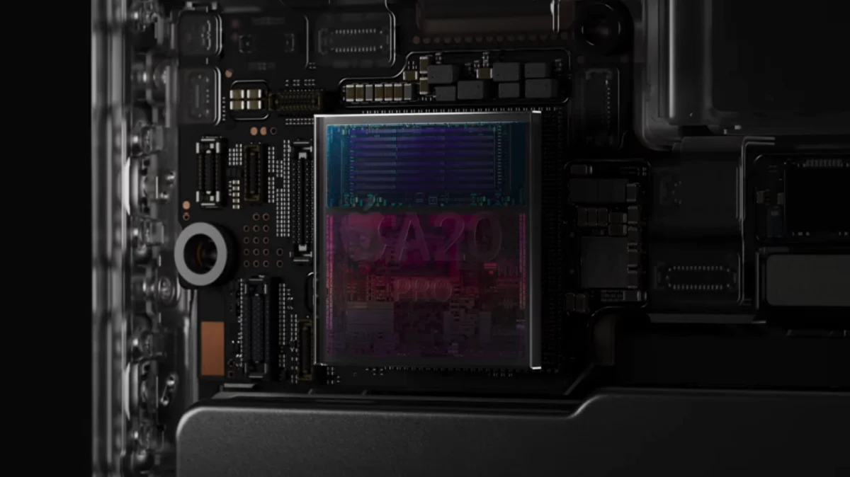
The evolution of mobile silicon has reached a historical milestone with the introduction of the A20 Pro chip, the beating heart of the iPhone 18 Pro and 18 Pro Max. To understand the sheer density of this engineering achievement, one must visualize the scale: the average human hair measures between 50 and 120 micrometers in width. If one were to take a mere 0.005 inches of that width and divide it by 63,500, the resulting figure is 2 nanometers. This is the precise scale at which the transistors within the A20 Pro are fabricated, representing a leap in miniaturization that pushes the boundaries of current lithography technology.
The Architectural Evolution of the A20 Pro
The A20 Pro does not merely represent a iterative increase in clock speed; it marks a fundamental shift in System-on-Chip (SoC) architecture. Inspired by the design philosophy of Apple’s M-series silicon used in professional-grade MacBooks, the A20 Pro integrates memory directly alongside the main silicon die. This physical restructuring is a strategic departure from traditional mobile SoC designs. By positioning the memory modules in immediate proximity to the processor, engineers have significantly reduced latency and improved thermal efficiency.

This design allows for more direct heat dissipation into the device’s internal vapor chamber, ensuring that the A20 Pro can sustain peak performance for longer durations without thermal throttling. Furthermore, the memory bandwidth has been elevated to an impressive 113.7 GB/s, a 50% increase over previous generations. This bandwidth is critical for handling the intensive computational demands of modern generative AI, high-fidelity gaming, and pro-grade video editing—tasks that previously were the exclusive domain of desktop workstations.
Chronology of Apple Silicon Advancements
To place the A20 Pro in its proper context, one must review the rapid maturation of Apple’s custom silicon over the last six years. The journey began in late 2020 with the M1 chip, which fundamentally disrupted the personal computing market by offering unprecedented performance-per-watt ratios.
- 2020: The M1 chip debuts, bringing Apple Silicon to the Mac lineup and setting a new benchmark for integrated processing.
- 2022–2024: A-series and M-series chips iterate through 5nm and 3nm processes, focusing on core count increases and neural engine efficiency.
- 2025: The M4 MacBook Air and iPhone 17 Pro define the "middle era" of high-efficiency, AI-ready mobile computing.
- 2026: The A20 Pro arrives on a 2nm process, effectively closing the performance gap between portable handheld devices and entry-level desktop machines.
This timeline reveals a consistent trend: the convergence of mobile and desktop computing architectures. The A20 Pro is the culmination of this convergence, utilizing the advanced cache structures and clock speeds once reserved for hardware requiring active cooling systems.

Comparative Performance Analysis
Recent Geekbench 6.7.x testing provides a rigorous quantitative look at how the A20 Pro stacks up against its predecessors and its desktop counterparts. The results are striking. The A20 Pro features a significantly boosted CPU clock speed, reaching an peak of 4.93 GHz, a substantial climb from the 4.26 GHz observed in the A19 Pro.
Perhaps most impressive is the expansion of the cache hierarchy. By increasing the L1 instruction cache, L1 data cache, and L2 cache, Apple has mitigated the "memory wall" that often limits processor performance. In head-to-head benchmarking against the M1 MacBook Air, the A20 Pro demonstrates more than double the single-core CPU and Metal GPU performance. When compared to the M4 MacBook Air, the A20 Pro nearly achieves parity in multi-core throughput.
For the end user, these numbers translate into real-world utility. Applications that once struggled with background processing on mobile devices now execute near-instantaneously. The "water pressure" analogy—often used by engineers to describe how a system handles sustained, high-intensity load—indicates that the A20 Pro maintains stability under conditions that would have forced older hardware into a lower power state within seconds.

Technical Implications and Industry Reaction
The transition to a 2nm process is not merely a marketing triumph; it is a significant engineering challenge. Managing electron leakage at the 2nm scale requires precise gate-all-around (GAA) transistor architectures. By successfully implementing this at scale, Apple has signaled to the broader semiconductor industry that the physical limitations of Moore’s Law are being pushed back, rather than hit.
While Apple has remained characteristically understated regarding the specifics of their manufacturing yields, industry analysts suggest that this design shift—moving the memory closer to the die—is a necessary response to the rising memory demands of on-device Large Language Models (LLMs). As smartphones become the primary interface for local AI processing, the demand for high-bandwidth, low-latency memory will only grow.
Market reactions have been largely positive, with supply chain analysts noting that the integration of memory alongside the SoC die reduces the overall footprint of the motherboard. This, in turn, allows for larger battery capacities or additional sensor arrays, reinforcing the "pro" designation of the iPhone 18 Pro series.

Broader Impact on Personal Computing
The existence of a 2nm chip with desktop-class performance in a handheld form factor raises significant questions about the future of traditional computing. If an iPhone 18 Pro can perform at the level of a 2024-era MacBook Air, the distinction between "mobile" and "desktop" hardware becomes increasingly architectural rather than performative.
For developers, this means the barrier to entry for creating high-performance software for iOS is effectively removed. The A20 Pro provides a consistent, high-performance foundation that allows for complex software—such as real-time 3D rendering, scientific simulation, and advanced neural network inference—to run locally on the device.
Moreover, the focus on heat dissipation via the vapor chamber suggests a new era of "sustained-performance mobile computing." Historically, mobile devices were designed for "burst" performance, intended to complete short tasks quickly before cooling down. The A20 Pro, by contrast, is engineered for sustained workloads, effectively bridging the gap between a portable phone and a functional mobile workstation.

Conclusion: The Future of the A-Series
The A20 Pro represents a pivotal moment in hardware history. By achieving 2nm density, optimizing memory bandwidth to 113.7 GB/s, and re-engineering the SoC layout for thermal efficiency, Apple has moved the iPhone 18 Pro series into a new category of performance.
While benchmark numbers are merely indicators of potential rather than the entirety of the user experience, they provide a clear map of the trajectory of modern silicon. As we look toward the future, the integration of these technologies—higher cache density, refined lithography, and memory proximity—will likely become the industry standard for all high-performance mobile devices. The A20 Pro serves as a testament to the fact that the most significant innovations in computing are often those that occur at the nanometer scale, invisible to the eye but transformative in their impact on the digital landscape. As the industry moves forward, the focus will undoubtedly remain on maintaining this trajectory, ensuring that the hardware in our pockets remains capable of meeting the escalating demands of an increasingly digital world.