
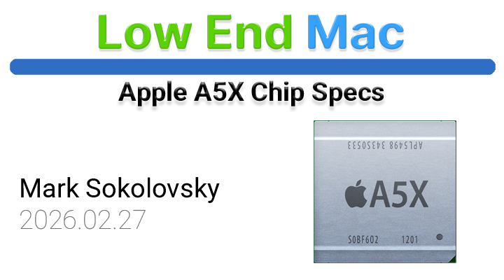
The Apple A5X System on a Chip (SoC) represents a significant milestone in Apple’s silicon development, particularly in its role powering the fourth-generation iPad. Released on March 16th, 2012, this dual-core processor, manufactured by Samsung using a 45-nanometer fabrication process, was designed to deliver enhanced graphical capabilities and improved overall performance for Apple’s flagship tablet. While the A5X shares its core architecture with its predecessor, the A5, its key differentiator lies in its significantly upgraded graphics processing unit (GPU) and memory subsystem, tailored to meet the demands of high-resolution displays and graphically intensive applications. This detailed hardware profile delves into the technical specifications of the A5X, offering insights into its architecture, performance potential, and the technological context of its release.
Core Architecture and Processing Power
At the heart of the Apple A5X SoC is a dual-core CPU based on the ARMv7 instruction set, operating in 32-bit mode. Each of these performance cores is clocked at 1 GHz, providing a robust foundation for handling a wide range of tasks, from everyday browsing and productivity to more demanding applications. The A5X does not feature efficiency cores, a design choice that prioritizes sustained performance over the power-saving heterogeneity seen in later Apple Silicon generations.
The cache hierarchy of the A5X is designed to facilitate rapid data access for its CPU cores. Each performance core is equipped with a 32 KB L1 instruction cache (L1i) and a 32 KB L1 data cache (L1d), totaling 64 KB of L1 cache per core. This per-core configuration ensures that each processing unit has immediate access to the data and instructions it needs, minimizing latency. Furthermore, the A5X features a unified 1 MB L2 cache for its performance cores. This shared L2 cache acts as a larger buffer for frequently accessed data, further accelerating processing by reducing the need to access slower main memory. The absence of specified efficiency cores means that there are no dedicated L1 or L2 caches for such cores, nor is there a system-level cache explicitly detailed in its architecture.
Memory Subsystem: A Key Upgrade for Graphics
The memory subsystem of the A5X was a critical area of enhancement compared to previous Apple SoCs. It utilizes a 128-bit memory bus, which is significantly wider than what was common in mobile processors of that era. This wider bus allows for a greater volume of data to be transferred between the SoC and its memory simultaneously. The memory controller supports four channels, each operating with a 32-bit width, contributing to the overall bandwidth.
The A5X is paired with LPDDR2 memory, specifically LPDDR2-800, which operates at a frequency of 400 MHz. This configuration results in an impressive theoretical memory bandwidth of approximately 12.8 GB/s. This substantial bandwidth was crucial for feeding the enhanced GPU with the large amounts of data required for rendering complex graphics and high-resolution displays. The total capacity of the RAM integrated with the A5X was 512 MB. This amount of memory, combined with the high bandwidth, was a key enabler for the Retina display technology introduced with the fourth-generation iPad, which boasted a resolution of 2048×1536 pixels.

Graphics Processing Power
The most significant upgrade in the A5X, and its namesake feature, is its graphics processing unit (GPU). While specific architectural details of Apple’s custom-designed GPUs are often proprietary, the A5X is understood to feature a quad-core GPU. This configuration is believed to include 8 SIMD (Single Instruction, Multiple Data) execution units, which are capable of performing operations on multiple data points simultaneously, a hallmark of efficient graphics processing.
These SIMD units, in turn, feed 64 FP32 (Floating Point 32-bit) Arithmetic Logic Units (ALUs). The FP32 ALUs are responsible for the complex mathematical calculations required for rendering 3D graphics, applying shaders, and processing image data. The GPU operates at a clock speed of 200 MHz, and this combination of cores, execution units, ALUs, and clock speed allows the A5X to achieve a theoretical peak performance of 25.6 GFLOPS (Giga Floating-point Operations Per Second). This level of graphical performance was a substantial leap forward, enabling smoother gameplay, more detailed visual effects, and improved responsiveness in graphically demanding applications. The A5X does not feature dedicated AI cores or AI processing capabilities, as artificial intelligence acceleration was not a primary focus for mobile SoCs at the time of its release.
Manufacturing and Release Context
The Apple A5X SoC was manufactured by Samsung, a long-standing fabrication partner for Apple’s custom silicon. The use of a 45-nanometer process technology at the time of its release was indicative of the leading edge of semiconductor manufacturing. This process node offered a balance between performance, power efficiency, and cost.

The A5X was officially released on March 16th, 2012, coinciding with the launch of the fourth-generation iPad. This device marked a significant upgrade over its predecessor, the iPad 2, which was powered by the A5 chip. The A5X was specifically designed to power the iPad’s Retina display, a feature that demanded a considerable increase in graphical horsepower and memory bandwidth to render its high pixel density. The A5X’s performance was particularly notable for its ability to handle 1080p video playback and complex 3D gaming, making the iPad a more compelling device for multimedia consumption and entertainment.
Technical Specifications Summary
| Feature | Specification |
|---|---|
| Name | Apple A5X |
| MFG | Samsung |
| Released | March 16th, 2012 |
| Codename | APL5498 |
| Part Number | S5L8945 |
| Fabrication Process | 45-Nanometer |
| Transistor Count | Not specified |
| CPU ISA | ARMv7 (32-Bit) |
| CPU Cores | 2 Performance Cores |
| CPU Clock Speed | 1 GHz |
| L1i Cache | 32 KB per-core (64 KB total) |
| L1d Cache | 32 KB per-core (64 KB total) |
| L2 Cache | 1 MB (Unified for Performance Cores) |
| Memory Bus Width | 128-Bit |
| Memory Channels | 4 |
| Memory Type | LPDDR2-800 (400 MHz) |
| Memory Bandwidth | ~12.8 GB/s |
| Memory Capacity | 512 MB |
| GPU Cores | 4 |
| SIMD EU | 8 |
| FP32 ALU | 64 |
| GPU Clock Speed | 200 MHz |
| FP32 (FLOPS) | 25.6 GFLOPS |
| AI Cores | Not specified |
| AI OPS | Not specified |
| iDevices Included | Fourth-generation iPad |
Impact and Implications
The Apple A5X was a crucial component in solidifying the iPad’s position as a leading tablet device. Its enhanced graphical capabilities directly addressed the user experience demands of the Retina display, which was a major selling point for the fourth-generation iPad. By providing the necessary processing power to render sharp, detailed visuals, Apple ensured that the tablet delivered on its promise of a visually immersive experience.
The increased memory bandwidth was equally important. It allowed the GPU and CPU to access the high-resolution display buffer and application data quickly, preventing bottlenecks that could lead to stuttering or lag. This focus on graphics and memory performance highlighted Apple’s strategy of optimizing its silicon for specific user experiences and device features.

While the A5X represented a significant leap, it also served as a stepping stone. The rapid pace of semiconductor development meant that even as the A5X powered the latest iPad, Apple was already working on its successors. The architectural decisions made in the A5X, particularly its emphasis on graphics and memory, would inform future generations of Apple Silicon, paving the way for even more powerful and efficient chips in subsequent iPads and other Apple devices. The A5X’s legacy lies in its successful integration of enhanced graphics and memory to support a groundbreaking display technology, setting a new standard for tablet performance and user experience at the time of its release. The data presented in this profile is sourced from public technical documentation and industry analysis, with a primary reference point being the comprehensive information available on Wikipedia’s Apple Silicon page, reflecting its status as a key component in the evolution of mobile processing.