Before Apple’s foray into custom silicon with the groundbreaking A4 chip in the iPhone 4, the early iOS devices relied on chips manufactured by Samsung. This strategic partnership laid the groundwork for the mobile computing revolution. However, a significant shift occurred with the first iPad, marking the beginning of Apple’s journey into designing its own System on a Chip (SoC) architecture, known as the "A-Series." This evolution, taking shape from 2010 onwards, has seen Apple’s chips become increasingly powerful and integrated, driving innovation across its product lines and reshaping the competitive landscape of the technology industry. By 2026, the iPhone 17 lineup showcases the A19 and A19 Pro chips, boasting desktop-class multicore processing, advanced graphical capabilities, and unparalleled responsiveness in smartphones and tablets. While current mobile Apple SoCs can rival chips like the M1, this remarkable progress is the culmination of years of incremental yet significant advancements.
The Genesis: Early Samsung-Based Silicon
The earliest iterations of Apple’s mobile devices were powered by chips that, while foundational, were primarily designed for power efficiency rather than raw performance. The initial prototypes of the iPhone even utilized Freescale i.MX31 chips. However, a crucial pivot occurred with the adoption of Samsung’s S5L89xx series.
The "APL0098" – The Apple A1 Chip
Known internally as "APL0098" and externally as the Samsung S5L8900, this chip was the heart of the very first iPhone, the original iPod touch, and the iPhone 3G. Developed with a focus on power efficiency, the S5L89xx chips represented a pragmatic approach to the nascent mobile market.
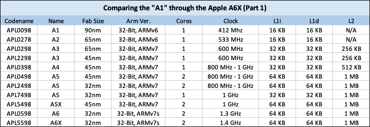
- Architecture: The A1 chip was a 32-bit ARMv6 processor.
- Fabrication: It was manufactured on a 90-nanometer process.
- Clock Speed: The chip was underclocked to 412 MHz from its default 666 MHz, a decision likely driven by thermal and battery life considerations.
- Cache: It featured 16 Kilobytes of Level 1 Instruction cache and another 16 KB for L1 data cache. Notably, it lacked L2, L3, or shared system caches.
- Cores: The A1 was a single-core processor.
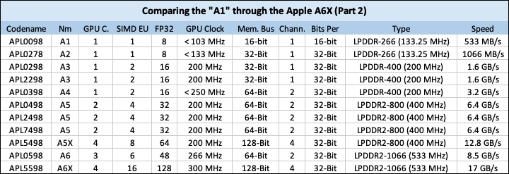
- Memory: It was equipped with 128 MB of 133.25 MHz LPDDR-266 RAM, resulting in a memory bandwidth of 533 MB/s.
The "APL0278" – The Unofficial Apple A2 Chip
While there was no officially designated "Apple A2" chip, the designation is fitting for the silicon used exclusively in the second-generation iPod touch. This chip shared significant similarities with the Apple A1 (S5L8900) but benefited from a more advanced manufacturing process.
- Fabrication: The A2 utilized a 65-nanometer process, a reduction from the A1’s 90nm. This smaller process node typically allows for improved power efficiency and potentially higher clock speeds.
- Improvements: While specific details are scarce, the transition to a smaller fabrication size suggests other optimizations and refinements were implemented.
The "S5L8920/S5L8922" – The Apple A3
The A3 series marked a notable step forward in performance, powering the iPhone 3GS and the third-generation iPod touch (S5L8922 variant). The key differentiator for the A3 was a significant enhancement in its cache architecture and memory capabilities.
- Cache Enhancements: The L1 Instruction and data caches were doubled to 32 KB per core, directly contributing to improved processing efficiency and responsiveness.
- Memory Bandwidth: Memory bandwidth was doubled to 1.6 GB/s, supported by 256 MB of LPDDR-400 (200 MHz) RAM. This increased bandwidth was crucial for handling more demanding applications and multitasking.
- GPU Boost: The maximum GPU clock speed was increased to 200 MHz, providing a noticeable uplift in graphical performance for games and visual applications.
- Introduction of L2 Cache: Crucially, the A3 chips introduced a 256 KB L2 cache. This was a significant architectural addition, as previous iOS devices lacked this level of cache, which helps to speed up access to frequently used data.
Apple’s In-House Revolution Begins: The A4 Chip
The introduction of the A4 chip in the iPhone 4 in 2010 represented a watershed moment for Apple. This was the company’s first custom-designed SoC, signifying a definitive move towards vertical integration and control over its hardware destiny.
The A4 Chip
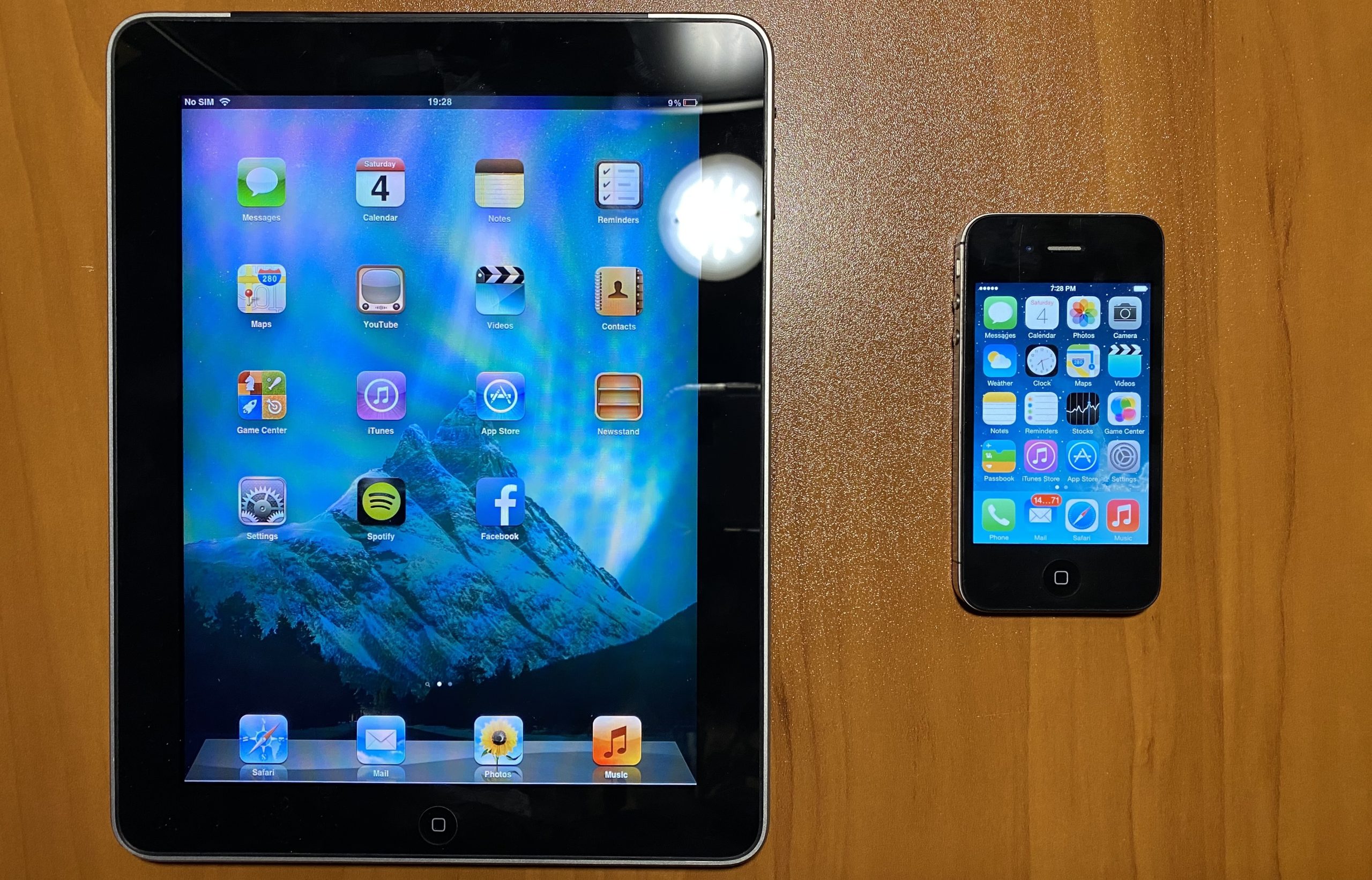
The A4 chip, much like the later M-series chips that would redefine personal computing, was Apple’s inaugural step into designing its own silicon. While still a 32-bit architecture, it powered the iPhone 4, the original iPad, and the fourth-generation iPod touch, delivering a significant leap in performance.

- Architecture: The A4 remained a 32-bit chip.
- CPU Clock Speed: Clock speeds were incrementally increased, ranging from 800 MHz to 1 GHz depending on the device.
- L2 Cache: The L2 cache was doubled to 512 KB, further enhancing data access speeds.
- Memory Bandwidth: Memory bandwidth saw a substantial increase to 3.2 GB/s across all devices utilizing this SoC.
Escalating Performance: The A5 and Beyond
The A5 generation marked a significant architectural shift, introducing dual-core processing and further enhancing graphical capabilities. This period also saw Apple exploring different manufacturing partners and refining its designs.
The A5 and A5X Chips
The A5 chip, introduced with the second-generation iPad in March 2011, was a dual-core processor that Apple claimed could "do twice the work" of the A4, with a ninefold increase in graphical performance. This represented a major leap in mobile processing power.
- Dual-Core Architecture: The A5 featured a dual-core CPU, significantly boosting multitasking and overall performance.
- Graphical Prowess: The graphics core also saw substantial improvements.
- L2 Cache: All A5 and A5X chips featured 1 MB of L2 cache, double that of the A4.
- Memory: Faster memory was integrated, improving overall system responsiveness.
- A5X Variant: The A5X, introduced with the third-generation iPad, was a higher-performance version of the A5. It featured a quad-core graphics chip, pushing graphical performance to an impressive 25.6 Gigaflops and incorporating numerous technical enhancements over the standard A5. Notably, the third-generation Apple TV used a locked-down single-core version of the A5, demonstrating Apple’s flexibility in tailoring chips for specific device needs.
The A6 and A6X Chips
The A6 and A6X chips, powering devices like the iPhone 5 and the fourth-generation iPad, continued the trend of performance escalation, notably breaking the 1 GHz CPU clock speed barrier.
- CPU Clock Speeds: The A6 reached 1.3 GHz in the iPhone 5/5c, while the A6X in the fourth-generation iPad hit 1.4 GHz.
- RAM Upgrade: The RAM was upgraded to LPDDR2-1066, providing a memory bandwidth of 8.5 GB/s for the A6 and an impressive 17 GB/s for the A6X.
- GPU Enhancements: The GPU clock speeds were also increased, with the A6X reaching 300 MHz compared to the A6’s 266 MHz.
A New Era: 64-Bit Computing and TSMC Partnership
The introduction of the A7 chip in September 2013 marked a pivotal moment: the arrival of the first 64-bit mobile Apple Silicon. This transition was not just a spec bump; it fundamentally changed how software could be developed and executed on mobile devices, paving the way for more complex applications and richer user experiences.
Apple A7: Kicking it Up a Notch
The A7 chip, featured in the iPhone 5s, iPad mini 2, iPad mini 3, and the original iPad Air, contained a staggering one billion transistors and utilized an even smaller fabrication process.
- 64-Bit Architecture: This was the first mobile chip to adopt a 64-bit architecture, enabling greater memory addressing capabilities and performance for demanding tasks.
- Transistor Count: The integration of one billion transistors signifies a massive increase in complexity and computational power.
- Fabrication Process: A smaller fabrication size further improved power efficiency and performance.
- Architectural Improvements: The A7 brought numerous architectural enhancements over its predecessors, leading to significant gains in CPU and GPU performance.
iPhone 6, 6 Plus, and the Apple A8
The iPhone 6 and 6 Plus, released in 2014, became incredibly popular, selling approximately a quarter of a billion units worldwide and becoming the most popular smartphones to date. This success was underpinned by the A8 chip.
- Performance Gains: The A8 chip provided a substantial performance boost, enabling smoother operation of the larger displays and more demanding applications.
- Popularity: The unprecedented sales figures for the iPhone 6 and 6 Plus highlight the success of Apple’s hardware and software integration at the time.
Apple A9, A9X, and the Rise of TSMC
The A9 and A9X chips, found in the iPhone 6s, 6s Plus, iPhone SE, and various iPad models, introduced further advancements and a significant shift in manufacturing.
- Dual Manufacturer Approach: Initially, the A9 chip was manufactured by Samsung, but Apple later introduced a TSMC-manufactured version for the iPhone SE. This dual-sourcing strategy allowed for greater production flexibility and potentially competitive pricing.
- DDR4 Adoption: The A9 was among the first Apple devices to utilize DDR4 memory, predating its adoption in Macs by about two years. This provided a significant increase in memory speed and efficiency.
- Custom Storage Solution: A major innovation was the inclusion of an Apple-designed NVMe controller, incorporating PCI Express. This resulted in significantly faster internal storage speeds for iPhones starting with the 6s, a critical component for quick app loading and data access.
Efficiency and Power: The A10 Fusion and Beyond
The A10 Fusion chip, introduced with the iPhone 7 and 7 Plus on September 16, 2016, heralded a new era of power efficiency and performance with its introduction of a quad-core design incorporating efficiency cores.
The A10 Fusion, A10X Fusion, and T2 Chip
The A10 Fusion was Apple’s first quad-core SoC, featuring two high-performance cores and two high-efficiency cores. This architecture allowed for a dynamic balance between power and battery life.
- Quad-Core Design: The A10 Fusion was the first Apple SoC to feature four cores, comprising two high-performance cores and two high-efficiency cores.
- Performance Uplift: Apple reported a 40% increase in CPU performance and a 50% increase in GPU performance over the A9.
- Efficiency Cores: The introduction of efficiency cores marked a significant step towards optimizing battery life without compromising performance for everyday tasks.
- A10X Fusion: This enhanced variant powered the third-generation iPad Pro, offering even greater CPU and GPU capabilities.
- T2 Chip: While not an A-series chip, the T2 Security Chip’s integration into Macs and other Apple devices around this time signaled Apple’s broader commitment to developing custom silicon for enhanced security and specialized functions.
The continuous evolution of Apple’s A-series chips, from their early reliance on external manufacturers to the development of highly integrated, custom-designed silicon, underscores a strategic vision focused on pushing the boundaries of mobile computing. Each iteration has brought significant improvements in processing power, graphical capabilities, and energy efficiency, consistently setting new benchmarks for the industry and reinforcing Apple’s position as a leader in technological innovation. The trajectory from the humble beginnings of the A1 chip to the anticipated power of the A19 and A19 Pro in 2026 demonstrates an unwavering commitment to delivering unparalleled performance and user experiences across its ecosystem.