 Vera Clarissa
Before Apple revolutionized the mobile landscape with its proprietary A-Series System on a Chip (SoC) designs, the company relied on third-party manufacturers, most notably Samsung, to power its groundbreaking iOS devices. The initial iterations of the iPhone and iPod touch featured chips sourced from Samsung, a partnership that laid the groundwork for the mobile computing revolution. However, with the introduction of the A4 chip in the iPhone 4, Apple embarked on a transformative journey, bringing its silicon design in-house and setting a new benchmark for performance and efficiency in the mobile industry. This strategic shift, beginning in 2010, marked the inception of the A-Series naming convention and has since become a cornerstone of Apple’s technological prowess, culminating in the highly anticipated A19 and A19 Pro chips powering the 2026 iPhone 17 lineup, which are projected to offer desktop-class multicore processing and graphical capabilities previously unimaginable in a smartphone.
The Genesis: From Samsung to the A1 Chip
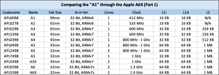
The earliest iOS devices, including the first-generation iPhone, iPod touch, and iPhone 3G, were powered by what can be retrospectively categorized as the "Apple A1" chip. Officially designated as "APL0098" or the Samsung S5L8900, this chip represented an early collaboration that prioritized power efficiency over raw performance. These chips were adopted after initial iPhone prototypes utilized Freescale i.MX31 processors, signaling Apple’s early exploration of optimal hardware solutions.
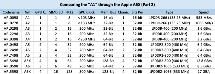
The S5L89xx series, based on the ARMv6 architecture, was a 32-bit chip manufactured using a 90-nanometer process. While its default clock speed was 666 MHz, it was often underclocked to 412 MHz for power conservation. Its cache configuration was modest by today’s standards, featuring 16 KB of Level 1 Instruction cache and another 16 KB for L1 data. Notably, it lacked any Level 2 or Level 3 cache, relying solely on a single processor core. Memory was handled by 128 MB of LPDDR-266 RAM running at 133.25 MHz, providing a memory bandwidth of 533 MB/s. This foundational chip, though basic by modern metrics, was instrumental in bringing the revolutionary iOS experience to consumers.
Iterative Improvements: The A2 and A3 Chips
While there isn’t an officially designated "Apple A2" chip, the designation is fitting for the processor used in the second-generation iPod touch. This chip, a variant of the A1, saw a significant manufacturing process shrink to 65nm, offering improved efficiency. Minor architectural tweaks also contributed to its performance.
The true evolutionary leap came with the S5L8920 and its variant S5L8922, often referred to as the "Apple A3" series. The S5L8920 powered the iPhone 3GS, while the S5L8922 was found in the third-generation iPod touch. These chips introduced key enhancements that boosted performance considerably. The L1 Instruction and data caches were doubled to 32 KB per core, a critical improvement for multitasking and application responsiveness. Memory bandwidth saw a substantial increase to 1.6 GB/s, supported by 256 MB of LPDDR-400 RAM operating at 200 MHz. Furthermore, the GPU clock speed was elevated to 200 MHz, and crucially, the A3 series marked the introduction of a 256 KB Level 2 cache, a feature absent in all previous iOS devices. This addition of L2 cache was a pivotal step in improving overall system performance and responsiveness.

The Dawn of In-House Silicon: The A4 Chip
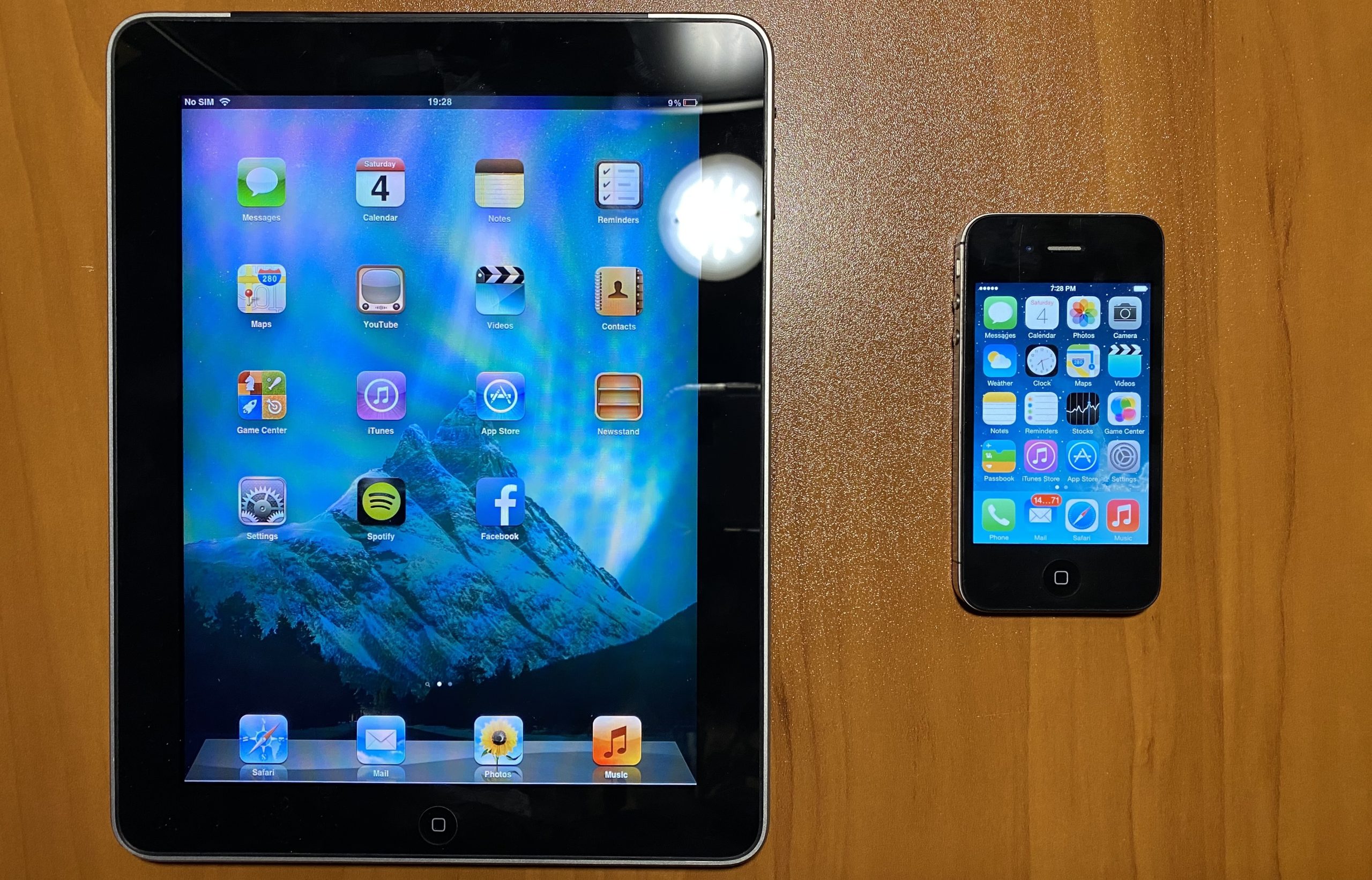
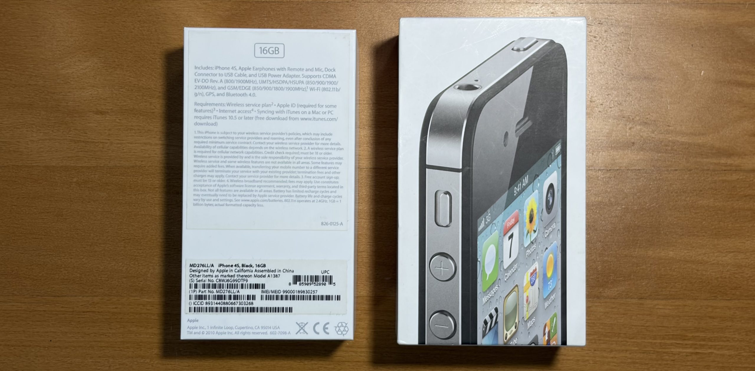
The year 2010 marked a watershed moment for Apple with the debut of the A4 chip, the company’s first custom-designed, in-house silicon. This chip, powering the iPhone 4, original iPad, and fourth-generation iPod touch, signaled Apple’s strategic pivot towards vertical integration and control over its hardware. The A4 represented a significant advancement over its predecessors, featuring a doubled L2 cache size to 512 KB.
CPU clock speeds were incrementally boosted, reaching up to 800 MHz in some devices and potentially touching 1 GHz in others. Memory bandwidth also saw a considerable increase, reaching 3.2 GB/s across devices equipped with the A4. This marked a critical transition for Apple, moving from relying on external chip designers and manufacturers to establishing its own formidable silicon design capabilities, a move that would profoundly shape its future product roadmap.

Expanding the Family: A5 and A5X Chips
The A5 chip, introduced in March 2011 with the second-generation iPad, was a significant step forward, boasting dual-core processing capabilities and a claimed doubling of workload capacity and a nine-fold increase in graphical performance compared to the A4. Apple advertised the A5 as capable of "doing twice the work," a testament to its enhanced architecture.
Technically, there were multiple iterations of the A5. While most were dual-core, a locked-down single-core version was developed specifically for the third-generation Apple TV. All A5 and A5X variants featured an improved 1 MB L2 cache, faster memory, and enhanced graphics cores. The A5X, introduced with the third-generation iPad, was a higher-performance variant specifically designed to drive the device’s Retina display. It incorporated a quad-core graphics chip, pushing graphical performance to approximately 25.6 Gigaflops and incorporating other technical improvements over the standard A5. This strategic differentiation in chip design allowed Apple to tailor performance to the specific needs of different devices within its ecosystem.

Pushing Boundaries: The A6 and A6X
The A6 and A6X chips represented further performance milestones, with CPU clock speeds finally surpassing the 1 GHz threshold. The A6 chip, found in the iPhone 5 and 5c, operated at 1.3 GHz, while the A6X, powering the fourth-generation iPad, reached 1.4 GHz. These chips also saw an upgrade in RAM technology to LPDDR2-1066, delivering impressive memory bandwidths of 8.5 GB/s for the A6 and a remarkable 17 GB/s for the A6X. The GPU clock speeds were also enhanced, with the A6 at 266 MHz and the A6X at 300 MHz. This progression demonstrated Apple’s continuous effort to optimize both processing power and memory throughput for a smoother user experience.
A Paradigm Shift: The 64-Bit A7 Chip
September 10th, 2013, heralded a new era with the introduction of the Apple A7 chip. This was a monumental achievement, as the A7 became the world’s first 64-bit mobile SoC. Integrated into the iPhone 5s, second and third-generation iPad mini, and the original iPad Air, the A7 chip packed a staggering one billion transistors and utilized an even smaller fabrication process. This architectural shift to 64-bit computing allowed for significantly larger memory addressability and more efficient processing of complex data, laying the groundwork for more sophisticated mobile applications and operating system features. The A7 marked a significant departure from the 32-bit architecture that had dominated mobile devices for years.
Popularity and Performance: The A8 Chip
The release of the iPhone 6 and 6 Plus in 2014 coincided with the introduction of the Apple A8 chip. These devices became incredibly popular, with the iPhone 6 and 6 Plus selling an estimated quarter of a billion units worldwide, making them the most successful iPhone models to date. The A8 chip continued Apple’s trajectory of incremental performance improvements, enhancing the user experience for a massive global user base. This period also saw Apple increasingly catering to consumer demand for larger screen sizes, a trend that the A8 helped to power effectively.
Diversification and Manufacturing: A9, A9X, and TSMC
The A9 and A9X chips, introduced with the iPhone 6s and 6s Plus, marked a significant diversification in manufacturing. While one version of the A9 was produced by Samsung, a nearly identical version was manufactured by Taiwan Semiconductor Manufacturing Company (TSMC). This dual-sourcing strategy, while intended to ensure supply, led to some debate among users regarding minor performance differences between the two variants. Crucially, the A9 series was the first Apple mobile platform to adopt DDR4 RAM, predating its implementation in Macs by approximately two years, showcasing Apple’s foresight in adopting cutting-edge memory technologies.
A key innovation within the A9 was its custom storage solution, featuring an Apple-designed NVMe controller. This integration of PCI Express technology led to substantially faster internal storage speeds on the iPhone 6s and subsequent models, a crucial upgrade that improved app loading times and overall device responsiveness. This move signaled Apple’s deep investment in optimizing every component of its devices, from the core processor to the storage subsystem.
Efficiency and Power: The A10 Fusion and Beyond
The iPhone 7 and 7 Plus, released on September 16th, 2016, introduced the A10 Fusion chip, a groundbreaking move that integrated four CPU cores: two high-performance cores and two high-efficiency cores. This "big.LITTLE" architecture, a concept pioneered by ARM, allowed the chip to dynamically switch between cores based on the task at hand, optimizing for both power consumption and performance. Apple claimed the A10 Fusion offered 40% better CPU performance and 50% more GPU performance than its predecessor, the A9.
Following the A10 Fusion, Apple continued its innovation with the A10X Fusion, designed for the 10.5-inch and 12.9-inch iPad Pro models. This chip further pushed the boundaries of tablet performance, offering enhanced multicore processing and graphics capabilities to handle demanding professional workflows. Concurrently, the T2 chip emerged, serving as a secure enclave processor in Macs, handling encryption, secure boot, and other critical security functions, demonstrating Apple’s expanding silicon expertise beyond mobile devices.
The Future: A Glimpse into 2026
Looking ahead, the trajectory of Apple’s silicon development is clear. By 2026, the iPhone 17 lineup is expected to feature the A19 and A19 Pro chips. Projections suggest these chips will deliver unprecedented levels of performance, rivaling desktop-class computing power. This continuous innovation underscores Apple’s commitment to pushing the boundaries of what is possible in mobile and personal computing, driven by its in-house silicon design capabilities. The journey from Samsung-manufactured chips to the highly advanced A-Series SoCs represents a remarkable testament to Apple’s engineering prowess and its strategic vision for controlling its technological destiny. The ongoing evolution of these chips not only defines the performance of Apple’s devices but also sets the pace for the entire technology industry.