 Vera Clarissa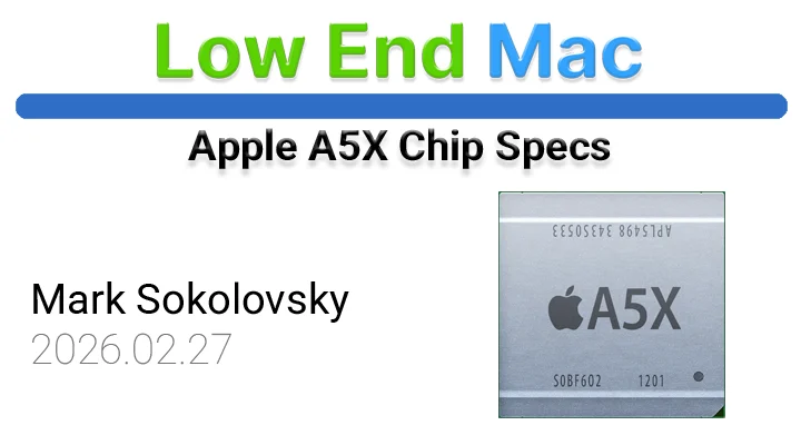
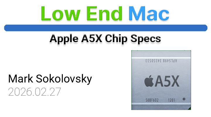
The Apple A5X System-on-Chip (SoC) represents a significant milestone in mobile processing, powering the revolutionary third-generation iPad, launched on March 16th, 2012. Manufactured by Samsung using a 45-nanometer fabrication process, this chip was engineered to deliver unprecedented graphics performance and overall system responsiveness, setting a new benchmark for tablet computing. The A5X is a testament to Apple’s vertical integration strategy, where the company designs its own silicon to optimize hardware and software synergy, a practice that has become a hallmark of its product ecosystem.
Genesis and Design Philosophy
The development of the A5X was intrinsically linked to Apple’s vision for the third-generation iPad. This iteration of the iPad was not merely an incremental update; it was a leap forward, most notably with the introduction of the Retina display. This high-resolution screen, boasting a staggering 2048×1536 pixel count, required a substantial increase in graphical processing power to render content smoothly and efficiently. The A5X was specifically designed to meet this demand, acting as the digital engine that brought the Retina display’s visual fidelity to life.
Apple’s approach to chip design at this time was characterized by a focus on dual-core CPU architectures coupled with increasingly sophisticated GPU components. The A5X followed this trend, building upon the foundation laid by its predecessors. While the A5 chip, found in the iPhone 4S and iPad 2, featured a dual-core ARM Cortex-A9 CPU, the A5X significantly enhanced the graphics capabilities. This strategic decision underscored Apple’s understanding that for an immersive visual experience, particularly with high-resolution displays and demanding applications, a robust GPU was paramount.
Technical Architecture and Key Specifications
The Apple A5X is an ARMv7-based SoC, operating on a 32-bit instruction set architecture. Its core components include a dual-core CPU and a quad-core GPU.
Central Processing Unit (CPU)
The CPU of the A5X features two high-performance cores, each clocked at approximately 1 GHz. These cores are based on the ARM Cortex-A9 architecture, known for its efficiency and performance in mobile applications. While Apple doesn’t typically disclose the exact transistor count for its chips at this level of detail, the complexity of the A5X suggests a significant number of transistors to accommodate its advanced features. The cache hierarchy includes 32 KB of L1 instruction cache and 32 KB of L1 data cache per core, totaling 64 KB of L1 cache per core. Furthermore, a shared 1 MB L2 cache is available for both CPU cores, facilitating faster data access and improving overall processing efficiency. The absence of dedicated efficiency cores in the A5X design indicates a focus on raw performance for demanding tasks, rather than the hybrid architecture that would become more prevalent in later Apple Silicon generations.

Graphics Processing Unit (GPU)
The most substantial upgrade in the A5X compared to its predecessor lies in its graphics processing capabilities. The A5X boasts a quad-core GPU, a significant increase from the dual-core GPU found in the A5. This GPU is characterized by 8 SIMD (Single Instruction, Multiple Data) execution units and 64 FP32 (Single-Precision Floating-Point) Arithmetic Logic Units (ALUs). Operating at a clock speed of approximately 200 MHz, the GPU delivers an estimated 25.6 GFLOPS (Giga Floating-point Operations Per Second). This raw computational power was crucial for rendering the high-resolution Retina display, enabling smooth scrolling, high-fidelity gaming, and accelerated video playback. The increased GPU cores and architectural enhancements were specifically tailored to handle the pixel density of the new display, ensuring that the iPad remained a fluid and responsive device for visual tasks.
Memory System
The memory subsystem of the A5X is a critical component contributing to its performance. It features a 128-bit wide memory bus, operating with four channels, each 32 bits wide. This configuration utilizes LPDDR2 SDRAM, specifically LPDDR2-800, running at a frequency of 400 MHz. This memory architecture allows for a theoretical memory bandwidth of approximately 12.8 GB/s. The A5X is equipped with 512 MB of RAM. This substantial bandwidth and capacity were essential for feeding the powerful CPU and, more importantly, the quad-core GPU with the data required for high-resolution graphics rendering and multitasking. The efficient management of memory bandwidth is a key factor in preventing bottlenecks, especially when dealing with graphically intensive applications and the demands of a high-resolution display.
Manufacturing and Timeline
The Apple A5X was manufactured by Samsung, a long-standing partner of Apple in semiconductor production. The chip was produced using a 45-nanometer process technology. This advanced manufacturing node at the time allowed for greater transistor density and improved power efficiency compared to older processes. The release date of March 16th, 2012, coincided with the launch of the third-generation iPad, a device that heavily relied on the A5X’s capabilities to differentiate itself in the burgeoning tablet market. The codename "APL5498" and part number "S5L8945" are internal identifiers used by Apple and its manufacturing partners to track and manage the chip during its development and production lifecycle.

The A5X in Context: Powering the Retina Display Revolution
The introduction of the third-generation iPad with its Retina display was a watershed moment for mobile computing. While previous iPads offered a good user experience, the leap in pixel density with the Retina display was transformative. This meant that text was sharper, images were more detailed, and the overall visual experience was significantly enhanced. However, this visual upgrade came with a considerable computational cost. The A5X was the direct response to this challenge. Its enhanced GPU architecture and broader memory bandwidth were precisely what was needed to drive the 3.1 million pixels of the Retina display without compromising performance.
The A5X wasn’t just about raw power; it was about enabling a specific user experience. The ability to run graphically demanding apps, play high-fidelity games, and consume high-definition video content smoothly on a tablet screen of that resolution was a significant achievement. This positioned the iPad as a serious contender not just for media consumption but also for productivity and even creative tasks. The A5X ensured that the visual fidelity of the Retina display was not a mere aesthetic feature but a functional enhancement that improved the usability and appeal of the device.
Performance Implications and Market Impact
The A5X processor was instrumental in the success of the third-generation iPad. It provided a tangible performance advantage, particularly in graphics-intensive applications, which helped Apple maintain its dominant position in the tablet market. The chip’s ability to handle the demands of the Retina display contributed to the device’s positive reception and strong sales figures.

From a broader industry perspective, the A5X, alongside other Apple Silicon advancements, signaled a shift in how powerful mobile devices could be. It demonstrated the potential of custom-designed SoCs to optimize performance for specific hardware and software ecosystems. This spurred further innovation across the industry, encouraging competitors to invest more heavily in their own chip development and optimization efforts. The focus on graphics performance also highlighted the growing importance of visual computing in mobile devices, paving the way for more sophisticated mobile gaming, augmented reality, and advanced visual applications.
Limitations and Evolution
While the A5X was a powerful chip for its time, it also represented a specific point in Apple’s technological evolution. The dual-core CPU architecture, while capable, would eventually be superseded by more advanced multi-core designs. The reliance on a 45-nanometer process, while leading-edge in 2012, would give way to smaller and more efficient manufacturing nodes in subsequent generations.
The evolution of Apple Silicon is a continuous process. Following the A5X, Apple introduced the A6X, which further boosted CPU and GPU performance, and continued to refine its architecture with each subsequent generation. The A5X, however, remains a crucial chapter in this narrative, showcasing Apple’s commitment to pushing the boundaries of mobile processing to enhance user experience and define new standards in portable computing.

Conclusion
The Apple A5X System-on-Chip was more than just a component; it was the engine that powered a revolution in tablet computing. Its robust dual-core CPU and significantly enhanced quad-core GPU were meticulously engineered to complement the groundbreaking Retina display of the third-generation iPad. Launched on March 16th, 2012, and manufactured by Samsung using a 45-nanometer process, the A5X delivered unprecedented graphical performance, enabling a visually stunning and highly responsive user experience. This chip underscored Apple’s strategic advantage in designing its own silicon, allowing for seamless integration of hardware and software. The A5X’s impact extended beyond the device it powered, setting new expectations for mobile performance and influencing the trajectory of the entire semiconductor industry. As a pivotal step in Apple’s ongoing innovation in custom silicon, the A5X stands as a testament to the company’s relentless pursuit of performance and user-centric design.
Source: (Apple Silicon, Wikipedia, the free encyclopedia, https://en.wikipedia.org/wiki/Apple_silicon, February 27th, 2026.)