 Vera Clarissa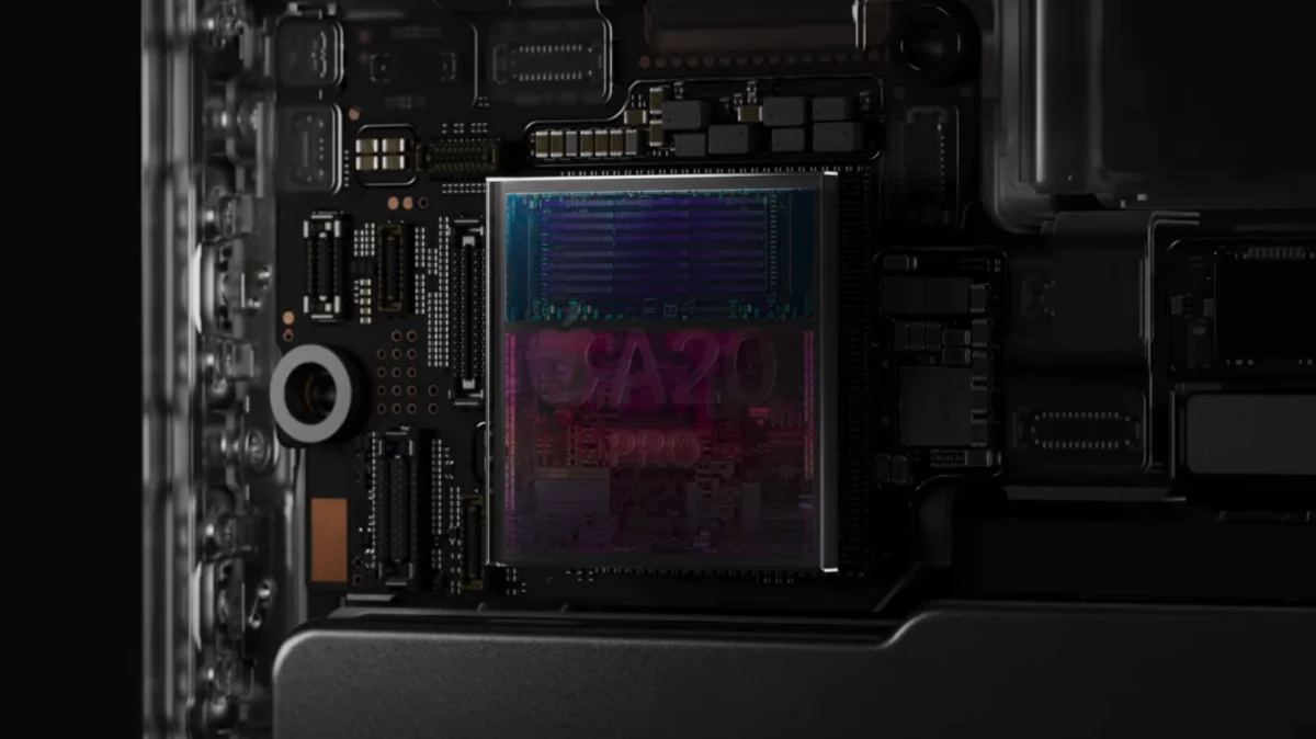
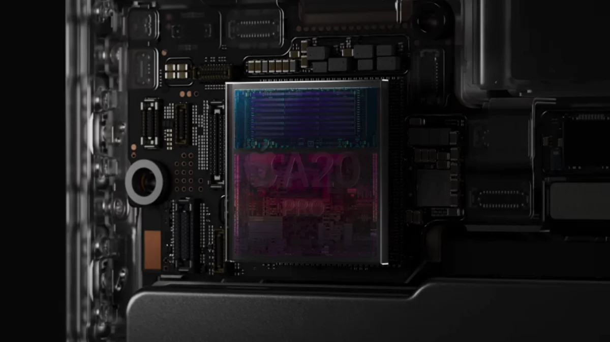
The A20 Pro chipset, powering the newly unveiled iPhone 18 Pro and Pro Max, represents a monumental shift in mobile semiconductor engineering by transitioning to a 2nm manufacturing process. To visualize the scale of this technological leap, consider that the average width of a human hair spans between 50 and 120 micrometers. When one divides a mere 0.005 inches—roughly the thickness of a few sheets of paper—by 63,500, the resulting figure is 2 nanometers. This infinitesimal scale is now the canvas upon which Apple has etched the transistors of its latest silicon, pushing the boundaries of what is physically possible in a handheld device.
This advancement marks a departure from previous architectural constraints. By utilizing a physically redesigned System-on-a-Chip (SoC) inspired by the high-performance M-series architecture, Apple has moved the memory chips alongside the main silicon die. This spatial reconfiguration facilitates superior heat dissipation into the device’s vapor chamber, enabling more sustained performance under heavy computational loads. Furthermore, this internal redesign has unlocked a 50% increase in memory bandwidth, now reaching a staggering 113.7 GB/s.

The Evolution of Apple Silicon: A Chronological Overview
The journey to the A20 Pro began in earnest in 2020 with the introduction of the M1 chip, which fundamentally altered the landscape of personal computing by transitioning the Mac lineup from Intel processors to custom ARM-based silicon. At the time, the M1 was praised for its efficiency-to-performance ratio, setting a standard that competitors struggled to match for years.
Following the success of the M1, Apple adopted an iterative strategy for its A-series mobile chips. The A15, A16, A17 Pro, and A19 Pro chips each brought incremental gains in transistor density and power efficiency. The A19 Pro, which preceded the current generation, operated at a clock speed of 4.26 GHz. The A20 Pro now shatters that ceiling, running at an unprecedented 4.93 GHz. This evolution highlights a consistent trend: Apple has successfully scaled desktop-class performance into a chassis that fits in a user’s pocket, consistently shortening the gap between the iPhone and the MacBook.
Technical Specifications and Performance Metrics
The upgrades present in the A20 Pro extend beyond simple clock speed increases. Through a detailed analysis using Geekbench 6.7.x, the performance deltas between the iPhone 17 Pro, the new iPhone 18 Pro, and legacy devices like the M1 and M4 MacBook Air become clear.

The A20 Pro features expanded L1 instruction and data caches, alongside a larger L2 cache. These modifications reduce latency when the processor fetches data, allowing the chip to process complex instructions more fluidly. In head-to-head testing, the A20 Pro exhibits a single-core CPU performance and Metal GPU performance that is more than double that of the original M1 chip. Perhaps most impressively, the A20 Pro’s multi-core performance now closely mirrors that of the M4 MacBook Air, signaling that the mobile flagship has officially reached parity with mid-range professional laptops.
The following data points summarize the architectural shifts:
- Process Node: 2nm (an industry-leading density).
- Clock Speed: 4.93 GHz (an approximate 15.7% increase over the A19 Pro).
- Memory Bandwidth: 113.7 GB/s (a 50% improvement over the previous generation).
- Cache Architecture: Expanded L1 and L2 capacities for optimized data throughput.
Benchmarking and Real-World Implications
While synthetic benchmarks such as Geekbench provide a standardized "water pressure test" for silicon, they represent only one facet of the user experience. In the context of modern mobile computing, these figures suggest that the A20 Pro is no longer limited by traditional "mobile" tasks. Instead, it is being positioned to handle intensive workflows such as real-time 8K video rendering, console-quality gaming with hardware-accelerated ray tracing, and on-device generative artificial intelligence tasks.

Industry analysts suggest that by relocating the memory closer to the silicon die, Apple has effectively mitigated the "thermal throttling" that often plagues high-performance mobile devices. By increasing the efficiency of the heat path, the system can maintain its peak 4.93 GHz clock speed for longer durations, which is critical for users who rely on their smartphones for professional-grade content creation.
Official Positioning and Industry Reaction
Apple’s messaging surrounding the iPhone 18 Pro event emphasized "desktop-class power in a mobile form factor." While official statements remain focused on the user experience—noting improvements in battery life despite the higher clock speeds—third-party engineers have pointed to the 2nm transition as the primary driver of this efficiency.
The integration of the memory alongside the die—a technique long used in the M-series Mac chips—indicates that Apple is standardizing its high-performance silicon design across its entire ecosystem. This creates a unified development environment where software written for the M4 can be ported to the A20 Pro with minimal friction. Developers in the gaming and creative sectors have already expressed optimism, noting that the increased bandwidth and cache sizes will allow for more complex assets and textures to be loaded into memory without taxing the system’s storage controller.

Broader Impact and Future Outlook
The release of the A20 Pro raises questions regarding the future of the laptop market. If the mobile chipset continues to track closely with the performance of mid-tier MacBook Air models, the functional divide between the smartphone and the laptop will continue to blur. For the average consumer, this means that the "bottleneck" in productivity is shifting away from hardware capability and toward software optimization and interface design.
Furthermore, the 2nm manufacturing process is a significant capital investment. As Apple continues to push the physical limits of silicon, the costs associated with fabrication are likely to rise, potentially influencing the pricing strategy for the iPhone Pro lineup in the coming years.
In conclusion, the A20 Pro is more than just an incremental upgrade to the iPhone hardware. It is a testament to the maturation of Apple Silicon, demonstrating that the company has mastered the art of power management and architectural design. By surpassing the M1 in nearly every metric and challenging the M4 in multi-core throughput, the A20 Pro sets a new benchmark for the industry. Whether this performance can be sustained across future iterations as physical limits are approached remains to be seen, but for the present, the iPhone 18 Pro stands as one of the most powerful computing devices ever produced.

As developers and users begin to integrate these chips into their daily workflows, the real-world impact will likely be felt in the rapid adoption of more sophisticated AI applications and high-fidelity mobile gaming, solidifying the iPhone’s role as the primary computing hub for a new generation of users. The shift to 2nm is not merely a numbers game; it is a fundamental transformation of the mobile experience, ensuring that the devices we carry are capable of tasks that, only a few years ago, required a desktop workstation.