 Vera Clarissa
Before Apple’s revolutionary foray into custom in-house silicon with the A4 chip in the iPhone 4, the foundational architecture of its early iOS devices relied on chips manufactured by Samsung. These early collaborations laid the groundwork for what would become a dominant force in mobile processing. Since the debut of the first iPad, every Apple device has proudly sported a chip engineered by Apple itself, known as the "A-Series" System on a Chip (SoC). This naming convention, adopted from 2010 onwards, signifies a profound shift in Apple’s hardware strategy, transitioning from reliance on third-party manufacturers to complete vertical integration of its core technologies.
Looking ahead to 2026, the iPhone 17 lineup is set to feature the ultra-powerful A19 and A19 Pro chips. These next-generation processors are poised to deliver desktop-class multicore processing, unparalleled graphical capabilities, and instantaneous responsiveness, fundamentally redefining the potential of smartphones and tablets. While current mobile Apple SoCs are already capable of rivaling established desktop processors like the M1, this remarkable advancement is the culmination of years of incremental innovation, a testament to Apple’s relentless pursuit of performance and efficiency.
The Genesis: "APL0098" and the Dawn of Apple Silicon
The very first chip to bear Apple’s silicon imprint, though manufactured by Samsung, was internally designated "APL0098." More commonly recognized as the Samsung S5L8900, this chip powered the groundbreaking original iPhone, the first-generation iPod touch, and the iPhone 3G. The adoption of the S5L89xx series followed an earlier exploration of Freescale i.MX31 chips for initial iPhone prototypes. At its inception, the S5L8900 was designed with a primary focus on power efficiency rather than raw performance, a crucial consideration for the nascent smartphone market.
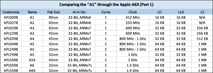
Technically, the "APL0098" was a 32-bit ARMv6 processor built on a 90-nanometer fabrication process. Its clock speed was intentionally throttled to 412 MHz, a reduction from its default 666 MHz. The chip featured a modest 16 Kilobytes of Level 1 Instruction cache and an equal amount for L1 data cache. Notably, it lacked any Level 2 or Level 3 cache, relying solely on its single processor core. Memory capabilities were equally rudimentary by today’s standards, comprising 128 MB of 133.25 MHz LPDDR-266 RAM, yielding a total memory bandwidth of approximately 533 MB/s.
The A2: A Subtle Iteration
While Apple never officially branded a chip as the "Apple A2," this designation is a fitting descriptor for the silicon used exclusively in the second-generation iPod touch. This chip, closely related to the A1’s S5L8900, represented a manufacturing refinement, moving to a more advanced 65nm process. Although specific details are scarce, this miniaturization likely contributed to improved power efficiency and potentially enhanced thermal management.

The A3: Doubling Down on Performance
The S5L8920 and its variant S5L8922 marked a significant evolutionary leap, powering the iPhone 3GS and the third-generation iPod touch, respectively. The primary differentiator between the A3 series and its predecessors was the doubling of Level 1 caches, increasing to 32 KB per core for both instruction and data. This enhancement directly contributed to a noticeable uplift in overall performance.
Memory bandwidth saw a substantial increase, doubling to 1.6 GB/s, supported by 256 MB of LPDDR-400 (200 MHz) RAM. This provided a more robust foundation for multitasking and demanding applications. The maximum GPU clock speed was also elevated to 200 MHz, and critically, the A3 series introduced the long-awaited 256 KB of Level 2 cache. This addition was a pivotal moment, as previous iOS devices lacked any L2 cache, highlighting Apple’s increasing focus on optimizing the entire processing pipeline.

The A4: The First In-House Design
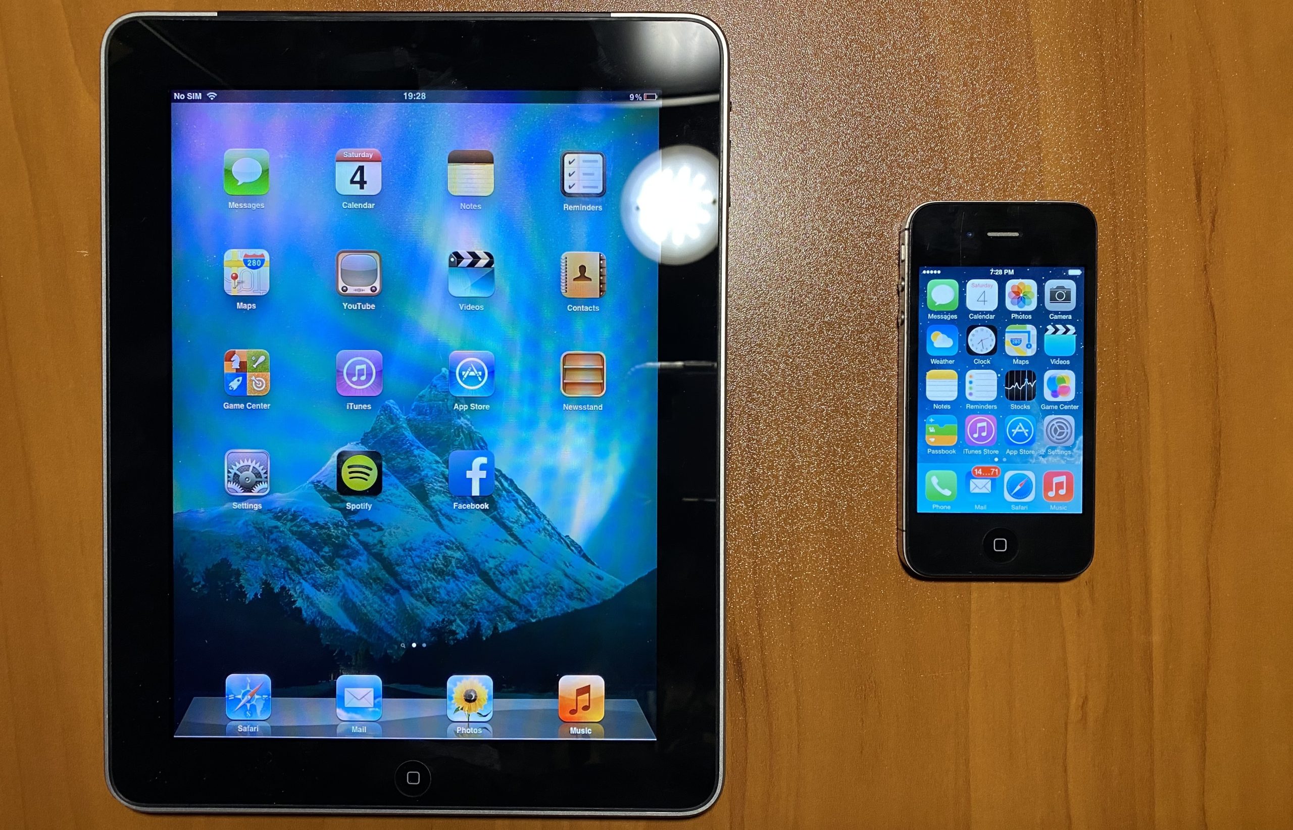
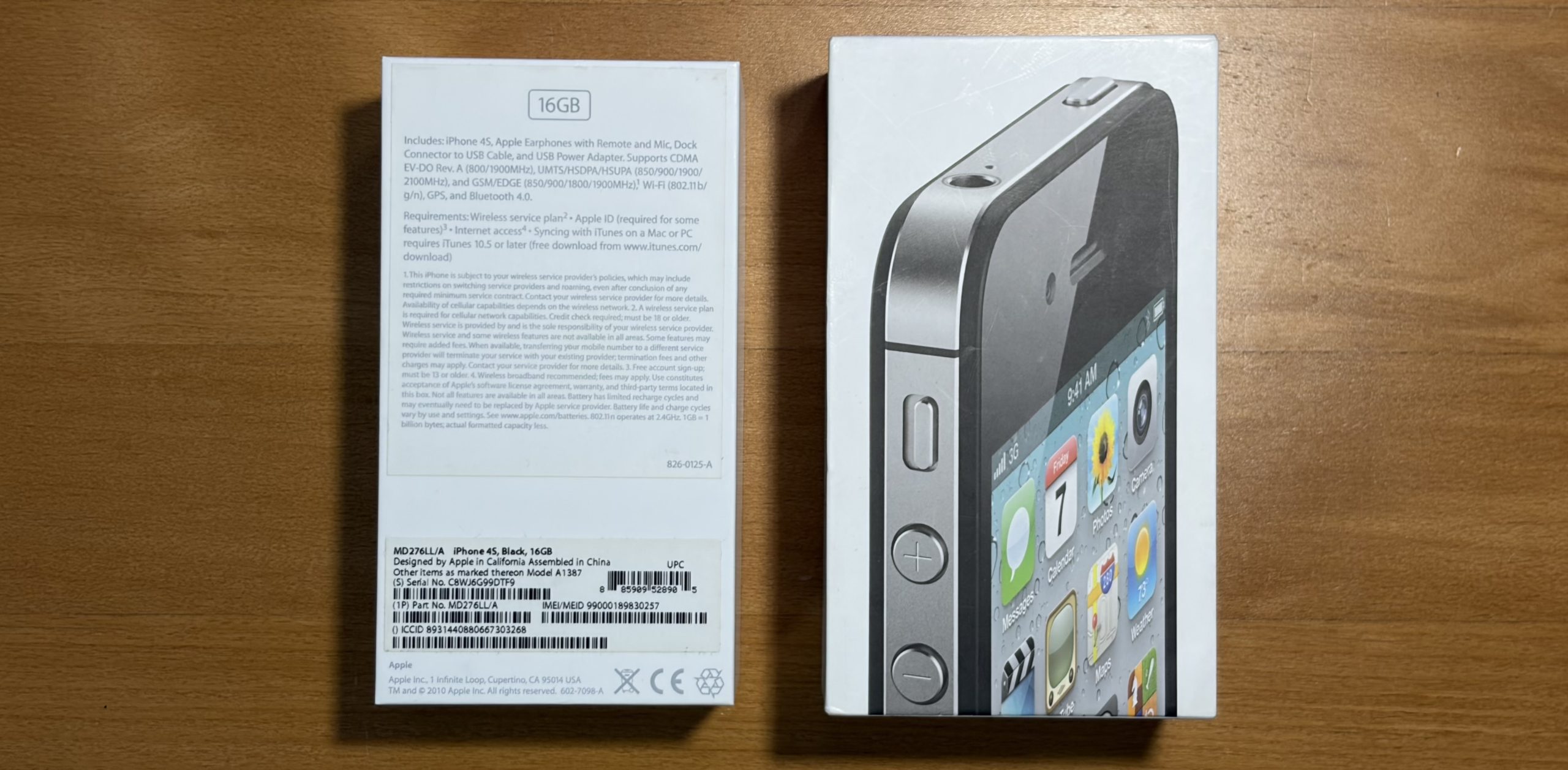
The introduction of the A4 chip in the iPhone 4 in 2010 represented a watershed moment: Apple’s first truly custom-designed SoC, mirroring the philosophy behind its later M-series chips. While still a 32-bit processor, the A4 powered a generation of iconic devices, including the iPhone 4, the original iPad, and the fourth-generation iPod touch.
Building upon the A3’s advancements, the A4 doubled the L2 cache to 512 KB. CPU clock speeds saw a modest increase, ranging from 800 MHz to 1 GHz depending on the device. Memory bandwidth was further enhanced to 3.2 GB/s across all devices utilizing this SoC. This shift towards in-house design signaled Apple’s commitment to controlling its hardware destiny, enabling tighter integration between hardware and software and paving the way for future performance breakthroughs.

The A5 Family: Dual-Core Power and Graphics Prowess
The A5 chip, launched in March 2011 with the second-generation iPad, was hailed by Apple as capable of "twice the work" of the A4, with a staggering nine-fold increase in graphical performance. The A5 architecture brought significant improvements in L2 cache, memory speed, and graphics processing.
Interestingly, the A5 family encompassed several variations. While most A5 chips were dual-core, a locked-down single-core version was developed specifically for the third-generation Apple TV. All A5 and A5X variants featured a 1 MB L2 cache.
The A5X, introduced with the third-generation iPad, represented a higher-performance iteration of the A5. It boasted a quad-core graphics chip, pushing graphical performance to an impressive 25.6 Gigaflops and incorporating several technical enhancements over its A5 counterpart. This strategic differentiation allowed Apple to tailor performance to specific product needs, optimizing both user experience and cost-effectiveness.
The A6 and A6X: Pushing Clock Speeds and Memory Bandwidth
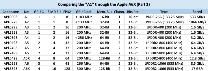
The A6 and A6X chips, found in devices like the iPhone 5, iPhone 5c, and the fourth-generation iPad, finally breached the 1 GHz CPU clock speed barrier. The iPhone 5 and 5c featured chips clocked at 1.3 GHz, while the A6X in the fourth-generation iPad reached 1.4 GHz.
The memory subsystem also saw upgrades, with LPDDR2-1066 (533 MHz) RAM delivering a memory bandwidth of 8.5 GB/s for the iPhones and a substantial 17 GB/s for the fourth-generation iPad. The GPU clock speeds were also refined, with the A6X on the iPad reaching 300 MHz compared to the 266 MHz found in the iPhone 5/5c. These incremental, yet impactful, improvements underscored Apple’s continuous refinement of its mobile silicon.
The A7: A 64-Bit Revolution
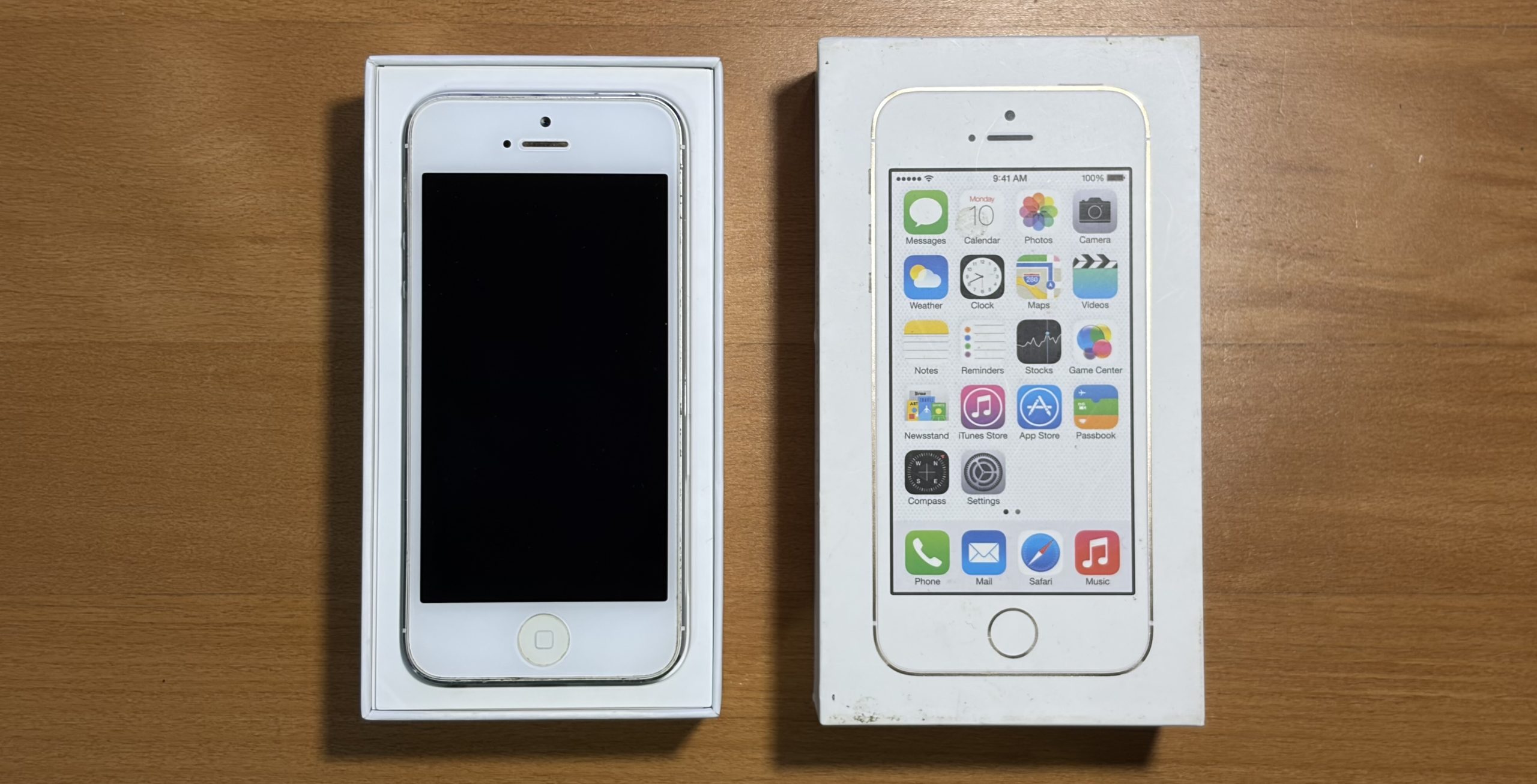
September 10th, 2013, marked a pivotal moment in mobile computing with the introduction of the Apple A7 chip alongside the iPhone 5s. This was the world’s first 64-bit mobile SoC, a groundbreaking architectural shift that would influence the entire industry. The A7 also found its way into the second and third generations of iPad mini, as well as the original iPad Air.
Featuring a staggering one billion transistors and a further reduced fabrication size, the A7 delivered a significant performance uplift over its predecessors. This architectural shift to 64-bit processing not only enabled more complex computations but also laid the groundwork for future software advancements that could leverage larger memory address spaces and more sophisticated instruction sets.
The A8: Riding the Wave of Popularity
The iPhone 6 and 6 Plus, released in 2014, were accompanied by the Apple A8 chip. These devices achieved unprecedented popularity, selling approximately a quarter of a billion units worldwide and becoming the most popular smartphones to date. The A8, while building on the A7’s foundation, continued Apple’s trajectory of performance enhancement and power efficiency. This era also saw the development of custom storage solutions integrated into the SoC, foreshadowing the advancements in storage speeds that would characterize future iPhones.
The A9 and A9X: TSMC Enters the Fray and DDR4 Adoption
The A9 and A9X chips, introduced with the iPhone 6s and 6s Plus, represented a significant evolution, marked by the introduction of a new manufacturing partner: TSMC (Taiwan Semiconductor Manufacturing Company). While two nearly identical versions of the A9 chip existed – one manufactured by Samsung and another by TSMC, which found its way into the iPhone SE – this marked a strategic diversification for Apple’s supply chain.
Crucially, the A9 was among the first Apple devices to adopt DDR4 memory, predating its appearance in Macs by approximately two years, where it was not seen until the 2017 5K iMac. This adoption of faster memory technology directly contributed to improved performance across the board.
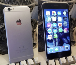
Furthermore, the A9 chip introduced a custom storage solution featuring an Apple-designed NVMe controller, leveraging PCI Express. This integration significantly accelerated internal storage speeds, a critical improvement that began to define the iPhone 6s and subsequent models, enhancing app loading times and overall system responsiveness.
The A10 Fusion and A10X Fusion: Efficiency Cores and Quad-Core Power
September 16th, 2016, saw the release of the iPhone 7 and 7 Plus, powered by the A10 Fusion. This chip was notable for introducing what is now a ubiquitous feature: Efficiency Cores. The A10 Fusion was Apple’s first quad-core SoC, boasting a reported 40% increase in CPU performance and a 50% boost in GPU performance over the A9, according to Apple’s own benchmarks. The integration of high-performance cores alongside power-efficient cores allowed for dynamic workload management, optimizing battery life without compromising on peak performance.
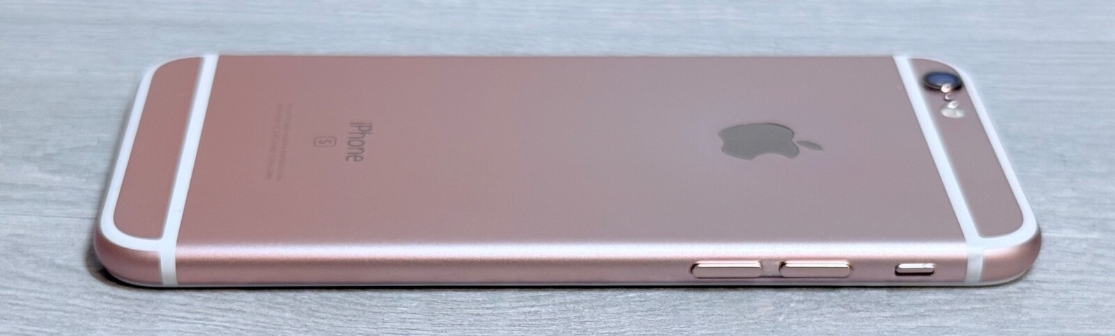
The A10X Fusion, found in devices like the third-generation iPad Pro, further pushed the boundaries of mobile processing. This iteration typically featured a higher core count for both CPU and GPU, delivering even greater computational power for demanding professional applications and high-end gaming.
The T2 Chip: A Dedicated Security and Control Hub
While not part of the A-series lineage, the T2 chip, introduced in later MacBook Pro models and other Macs, deserves mention for its impact on Apple’s integrated silicon strategy. The T2 chip served as a dedicated security processor, handling tasks such as secure boot, encryption, and Touch ID authentication. It also managed audio and SSD control, offloading these functions from the main CPU and contributing to overall system efficiency and security. This demonstrated Apple’s broader commitment to designing specialized silicon for critical functions across its product ecosystem.
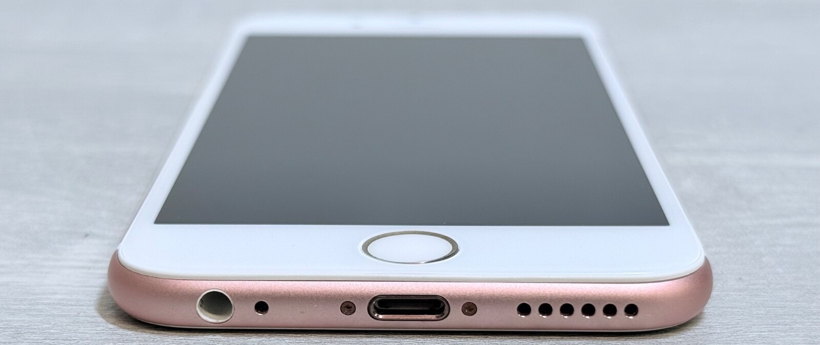
The journey from Samsung-supplied chips to Apple’s own highly integrated A-series processors represents a remarkable technological evolution. Each generation has brought significant advancements in performance, efficiency, and feature sets, solidifying Apple’s position as a leader in mobile silicon design and setting the stage for future innovations that continue to push the boundaries of what’s possible with personal computing devices.