 Vera Clarissa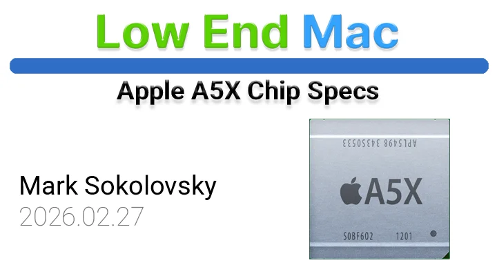
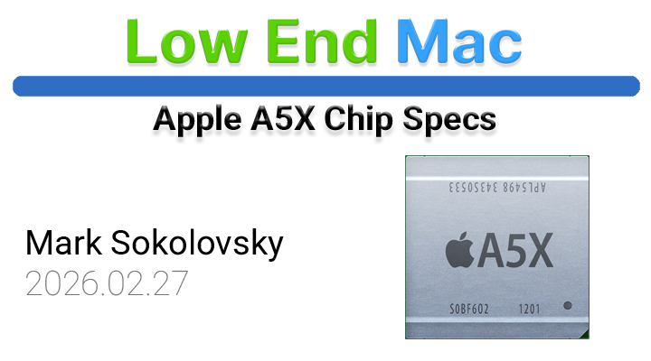
The Apple A5X System on a Chip (SoC) represents a significant milestone in Apple’s silicon development, powering a generation of iconic devices that redefined mobile computing. This detailed examination delves into the A5X’s intricate hardware profile, tracing its lineage, dissecting its core components, and understanding its contribution to the technological landscape of its era. Manufactured by Samsung, the A5X was officially released on March 16th, 2012, carrying the internal codename APL5498 and part number S5L8945. Built on a 45-nanometer fabrication process, this SoC was engineered to deliver enhanced performance, particularly in graphics, for Apple’s burgeoning tablet and smartphone offerings. While the precise transistor count remains undisclosed by Apple, its architectural innovations laid the groundwork for subsequent advancements in mobile processing.
Architectural Foundation and CPU Performance
The A5X chip adheres to the ARMv7 instruction set architecture, operating in a 32-bit environment. At its heart lies a dual-core CPU configuration, both cores designed for performance. Each of these "Performance Cores" (P-Cores) operates at a clock speed of 1 GHz. Notably, the A5X did not feature efficiency cores (E-Cores) or their associated clocks, a design choice that prioritized raw processing power over power efficiency in its target applications. This dual-core setup provided a substantial uplift in computational capabilities compared to its predecessors.
The cache hierarchy within the A5X was meticulously designed to minimize latency and maximize data throughput for the CPU. Each performance core was equipped with a 32 KB L1 instruction cache (L1i) and a 32 KB L1 data cache (L1d), totaling 64 KB of L1 cache per core. These dedicated caches ensured that frequently accessed instructions and data were readily available, significantly speeding up processing cycles. Furthermore, each performance core benefited from a 1 MB L2 cache, which was unified, meaning it served both instruction and data requests. The total L2 cache capacity for the CPU was therefore 1 MB. The absence of an explicit system-level cache in the disclosed specifications suggests a design where the L2 cache played a more dominant role in bridging the gap between the CPU cores and main memory. This architecture, while powerful for its time, also hinted at a focus on delivering immediate performance gains rather than the complex power-saving strategies seen in later SoC designs.
Memory Subsystem and Bandwidth
A critical component of any high-performance SoC is its memory subsystem. The A5X featured a robust memory configuration designed to keep its powerful CPU and GPU fed with data. The memory bus width was an impressive 128 bits, a significant figure that allowed for a substantial amount of data to be transferred simultaneously. This wide bus was further supported by a total of four memory channels, each operating at 32 bits. The memory type employed was LPDDR2-800, operating at an effective frequency of 400 MHz. This combination of wide bus, multiple channels, and fast memory type resulted in a theoretical memory bandwidth of approximately 12.8 GB/s. This substantial bandwidth was crucial for enabling smooth multitasking and handling demanding graphical workloads. The A5X was equipped with 512 MB of RAM, a capacity that, while modest by today’s standards, was commensurate with the devices it powered and the software capabilities of the era. The efficient utilization of this memory, coupled with the high bandwidth, allowed for a fluid user experience in visually rich applications and multitasking scenarios.
Graphics Processing Powerhouse
The graphics capabilities of the A5X were a major leap forward, particularly distinguishing it from its A5 predecessor. The A5X integrated a powerful GPU featuring four cores. These cores were further augmented by 8 SIMD (Single Instruction, Multiple Data) execution units and 64 FP32 (32-bit floating-point) Arithmetic Logic Units (ALUs). Operating at a clock speed of 200 MHz, the GPU was capable of delivering approximately 25.6 GFLOPs (Giga Floating-point Operations Per Second) of raw processing power. This significant increase in graphical horsepower was specifically engineered to handle the demands of higher-resolution displays and more graphically intensive applications, a key consideration for the tablet market where visual fidelity was increasingly becoming a differentiator. The A5X did not feature dedicated AI cores or AI operations metrics, as artificial intelligence processing was not a primary design focus for mobile SoCs in 2012. The emphasis was firmly on delivering a superior visual and computational experience.

Chronology and Context of Release
The release of the A5X in March 2012 was a pivotal moment for Apple’s mobile device strategy. It was primarily featured in the third-generation iPad, released in the same month. This tablet was lauded for its Retina display, a high-resolution screen that demanded a significant increase in graphics processing power to render content smoothly. The A5X, with its enhanced GPU, was the direct answer to this challenge, enabling the iPad to deliver sharper images, more detailed graphics, and a more immersive visual experience than any previous tablet on the market.
Prior to the A5X, Apple’s A-series chips, such as the A4 and A5, had steadily improved performance. The A5, released in the iPad 2 and iPhone 4S, was a dual-core processor that represented a significant step up from the single-core A4. However, the A5X was not merely an iterative update; it was a strategic architectural shift, particularly in its graphics capabilities, to meet the demands of a new generation of displays. This focus on graphics was a key differentiator for Apple, allowing its devices to excel in areas like gaming, media consumption, and professional creative applications.
The A5X’s debut also occurred during a period of intense competition in the mobile processor market. Qualcomm’s Snapdragon processors, NVIDIA’s Tegra chips, and Samsung’s own Exynos series were all vying for market share. Apple’s decision to design its own silicon, manufactured by partners like Samsung, allowed for a level of customization and optimization that was difficult for competitors to match. The A5X exemplified this advantage, showcasing Apple’s ability to tailor hardware to its software ecosystem and user experience goals.

Supporting Data and Performance Benchmarks
While specific benchmark scores for the A5X are not provided in the original data, historical context and device specifications offer insights into its performance. The third-generation iPad, powered by the A5X, was capable of rendering graphics at a resolution of 2048×1536 pixels, a substantial leap from the 1024×768 resolution of its predecessor. This Retina display boasted a pixel density of 264 pixels per inch, requiring the A5X’s enhanced GPU to drive such a detailed visual experience without lag.
In real-world use, the A5X facilitated smoother gameplay for demanding mobile titles, faster rendering of complex web pages, and improved performance in photo and video editing applications. Its dual-core CPU, while not the highest clock speed available at the time, offered a balanced performance profile for everyday tasks and multitasking, a crucial aspect of the tablet user experience. The 12.8 GB/s memory bandwidth was instrumental in ensuring that the CPU and GPU could access the necessary data quickly, preventing bottlenecks and contributing to the overall responsiveness of the device.
Official Responses and Market Implications
Apple, as is its practice, did not release extensive technical details about the A5X beyond its immediate impact on device performance. However, the company’s marketing and product launches consistently highlighted the graphical prowess and overall speed improvements brought by the A5X. The device itself, the third-generation iPad, was met with widespread critical acclaim, with reviewers frequently praising its stunning display and smooth performance, directly attributable to the A5X chip.

The A5X’s success had significant implications for the broader semiconductor and mobile device markets. It solidified Apple’s strategy of in-house silicon design, demonstrating that custom-designed SoCs could offer a distinct competitive advantage. This success likely influenced other manufacturers to invest more heavily in their own chip development or to seek closer collaborations with foundry partners to achieve similar levels of optimization. The emphasis on graphical performance also signaled a shift in the mobile industry, where visual fidelity and gaming capabilities were becoming increasingly important purchasing factors for consumers.
Broader Impact and Legacy
The Apple A5X chip, though no longer in production for new devices, leaves a lasting legacy. It was a crucial component in the evolution of the tablet computer, transforming it from a niche device to a mainstream entertainment and productivity tool. The A5X’s ability to power high-resolution displays and demanding applications set a new standard for mobile graphics performance and underscored the importance of integrated graphics processing in the overall user experience.
Its architectural decisions, particularly the focus on a powerful GPU alongside a capable dual-core CPU, provided a blueprint for subsequent Apple silicon designs. The emphasis on maximizing memory bandwidth and optimizing cache hierarchies were lessons that would be applied and refined in future A-series chips, leading to the even more powerful and efficient SoCs that power today’s iPhones, iPads, and Macs. The A5X stands as a testament to Apple’s engineering prowess and its commitment to pushing the boundaries of mobile technology, directly contributing to the creation of devices that shaped how millions of people interact with digital content and information. Its existence highlights a critical period in the mobile revolution, where hardware innovation directly fueled the expansion of software capabilities and user expectations.