 Vera Clarissa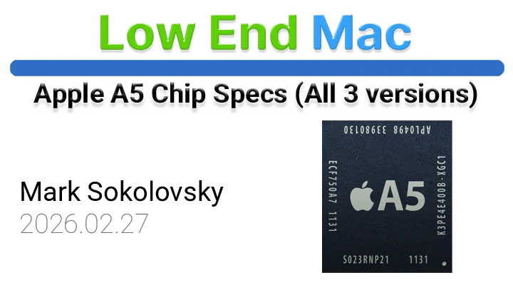
The Apple A5 chip, a dual-core system-on-a-chip (SoC) designed by Apple Inc., marked a significant advancement in mobile processing power upon its release. This article provides a comprehensive examination of the A5’s hardware profile, exploring its architecture, manufacturing process, performance capabilities, and its role in powering some of Apple’s most iconic devices during a pivotal era of smartphone and tablet evolution. The A5 was not a singular entity but rather a series encompassing three distinct variations, each tailored to specific product requirements, underscoring Apple’s commitment to iterative refinement and performance optimization.
Genesis and Evolution of the A5 Architecture
The A5 chip made its debut on March 11, 2011, integrated into the second-generation iPad. This launch signaled Apple’s continued ambition to push the boundaries of mobile computing, moving beyond the single-core architecture that had characterized its earlier A4 chip. The A5 was manufactured by Samsung, leveraging its advanced semiconductor fabrication capabilities. The initial iterations of the A5 were produced using a 45-nanometer process, with later revisions transitioning to a more efficient 32nm High-K dielectric metal gate process. This technological leap was crucial for enhancing performance while simultaneously improving power efficiency, a critical factor for battery-dependent mobile devices.
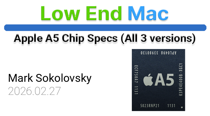
The A5’s codename, APL0498, and its part number, S5L8940, are technical identifiers that help trace its lineage within Apple’s chip development roadmap. While the exact transistor count for the A5 chip is not publicly detailed, its architectural complexity, featuring dual CPU cores and an integrated GPU, suggests a substantial increase over its predecessor. The chip’s CPU ISA (Instruction Set Architecture) is ARMv7, a 32-bit architecture widely adopted in mobile processors for its balance of performance and power efficiency.
Core Components and Performance Metrics
At the heart of the Apple A5 chip lies its dual-core CPU. These cores were designed for high performance, operating within a clock speed range of 800 MHz to 1 GHz. This dual-core configuration represented a significant leap from the single-core A4, enabling smoother multitasking, faster application loading, and more responsive user interfaces. Unlike later Apple Silicon designs that prominently feature dedicated efficiency cores, the original A5 configuration focused on two performance cores. However, a notable variation existed in the Apple TV (3rd generation), which utilized a single-core version of the A5. This adaptation demonstrates Apple’s strategy of tailoring chip designs to the specific needs and thermal envelopes of different product categories.
The A5’s cache hierarchy was also a critical component in its performance. Each performance core was equipped with 32 KB of L1 instruction cache (L1i) and 32 KB of L1 data cache (L1d), totaling 64 KB of L1 cache per core. For the dual-core configuration, this meant a total of 64 KB of L1i and 64 KB of L1d cache. The Apple TV (3rd generation) variant, with its single core, had a reduced L1 cache configuration of 32 KB for both L1i and L1d. Furthermore, the A5 featured a unified 1 MB L2 cache accessible by both performance cores, which significantly reduced memory access latency and boosted overall processing efficiency. The absence of dedicated efficiency cores and a system-level cache in the A5 design highlights the architectural priorities of its time, focusing on raw performance from its primary cores.
Graphics Capabilities and Memory Subsystem
The graphical prowess of the A5 was handled by an integrated PowerVR SGX543MP2 GPU. This dual-core GPU featured two shader cores, each with four SIMD (Single Instruction, Multiple Data) execution units, totaling eight SIMD cores. These cores were capable of processing 32 FP32 (single-precision floating-point) operations concurrently, leading to a theoretical peak performance of approximately 12.8 GFLOPS (Giga Floating-point Operations Per Second) at its 200 MHz clock speed. This graphical capability was instrumental in rendering smooth animations, supporting higher-resolution displays, and enabling more graphically intensive applications and games.
The memory subsystem of the A5 was equally crucial for its overall performance. It utilized an LPDDR2-800 memory type, operating at a frequency of 400 MHz. The memory bus width was 64 bits, configured as two 32-bit channels. This architecture provided a theoretical memory bandwidth of 6.4 GB/s, a substantial improvement that allowed the CPU and GPU to access data more rapidly. The A5 chip was typically paired with 512 MB of RAM. This memory capacity was sufficient for the operating systems and applications of the era, facilitating a fluid user experience on devices like the iPad 2 and iPhone 4S.
A Timeline of A5 Integration
The Apple A5 chip’s impact can be best understood by examining its deployment across key Apple products:

- March 2011: iPad (2nd generation) – The A5 chip made its grand debut within the iPad 2, offering a significant performance upgrade over its predecessor. This allowed for a more responsive tablet experience, with faster app loading and smoother multitasking, setting a new benchmark for tablet computing.
- October 2011: iPhone 4S – The A5 chip, likely a slightly refined version, powered the iPhone 4S. This integration brought dual-core processing to Apple’s flagship smartphone, dramatically enhancing its speed and responsiveness for everything from web browsing and gaming to camera operations and Siri, Apple’s revolutionary voice assistant.
- March 2012: Apple TV (3rd generation) – A single-core variant of the A5 chip was employed in the third-generation Apple TV. This adaptation demonstrated Apple’s ability to customize SoC designs for specific product needs, balancing performance with the thermal and power constraints of a set-top box.
- March 2012: iPad (3rd generation) – While the third-generation iPad primarily featured the A5X chip (an evolution with a more powerful GPU), some early or specific configurations might have retained elements or shared architectural foundations with the A5. However, the A5X was the main processor for this device, offering enhanced graphics for its Retina display.
The widespread adoption of the A5 across these influential devices underscores its success as a versatile and powerful mobile processor. It was a critical component in Apple’s strategy to deliver a premium user experience, differentiating its products in a rapidly evolving and competitive market.
Manufacturing and Technological Context
The partnership with Samsung for the A5’s fabrication was a testament to the symbiotic yet competitive relationship between the two tech giants at the time. Samsung’s advanced manufacturing facilities were essential for producing the complex dual-core A5 chips at scale and with high yields. The transition from a 45nm to a 32nm process was not merely a technical upgrade; it represented a significant step in miniaturization and energy efficiency. Smaller process nodes generally translate to lower power consumption and reduced heat generation, both critical for mobile devices that rely on battery power and are often held close to the user.
The "High-K dielectric metal gate" (HKMG) technology employed in the 32nm process was a crucial innovation. It allowed for thinner gate dielectrics and improved gate control, reducing leakage currents and further enhancing power efficiency. This technological advancement was not exclusive to Apple but was a general trend in leading-edge semiconductor manufacturing, and Apple’s adoption of it in the A5 showcased its commitment to leveraging the best available technology to optimize its hardware.

Implications and Legacy of the A5
The Apple A5 chip played a pivotal role in solidifying Apple’s reputation for delivering industry-leading performance in its mobile devices. Its dual-core architecture, coupled with a capable GPU and efficient memory subsystem, provided the horsepower necessary for the burgeoning mobile app ecosystem. Devices powered by the A5 were capable of handling more complex applications, richer multimedia experiences, and the increasingly sophisticated features of iOS, such as FaceTime video calling and the early iterations of Siri.
The A5’s success also laid the groundwork for Apple’s subsequent in-house chip development. By designing and controlling the architecture of its processors, Apple gained a significant competitive advantage, allowing it to optimize hardware and software integration for a seamless user experience. This vertical integration strategy, which began to take significant shape with the A4 and A5, has become a hallmark of Apple’s product development, enabling it to consistently deliver devices that are both powerful and efficient.
While the A5 has since been surpassed by more advanced Apple Silicon chips, its impact on the mobile industry remains undeniable. It was a key enabler of the tablet computing revolution and a significant contributor to the evolution of the smartphone from a communication device to a powerful, pocket-sized computer. The architectural choices made in the A5 – dual-core processing, integrated graphics, and efficient memory – became foundational elements for mobile chip design across the industry for years to come. Its story is a crucial chapter in the ongoing narrative of mobile technology, showcasing how targeted hardware innovation can drive significant leaps in user experience and redefine the capabilities of personal electronics. The A5 chip was not just a component; it was a catalyst that propelled the mobile revolution into a new era of performance and possibility.