 Vera Clarissa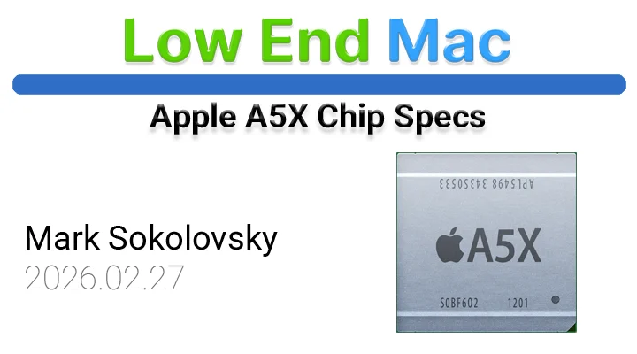
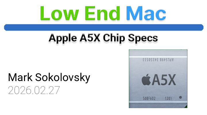
The Apple A5X System-on-Chip (SoC) represents a pivotal advancement in mobile processing technology, meticulously detailed in its hardware profile. Launched on March 16th, 2012, and manufactured by Samsung utilizing a 45-nanometer fabrication process, the A5X was a testament to Apple’s relentless pursuit of enhanced performance and graphical capabilities in its mobile devices. This SoC, codenamed APL5498 and bearing the part number S5L8945, was engineered to power the next generation of Apple’s tablet offerings, specifically the third-generation iPad, which was unveiled shortly after its release. Its architecture laid crucial groundwork for future innovations in Apple’s silicon development, influencing subsequent generations of A-series chips.
Architectural Overview: CPU and Memory Configuration
At the core of the A5X is a dual-core CPU architecture built upon the ARMv7 instruction set, operating in a 32-bit mode. Each of the two performance cores (P-Cores) clocked at a steady 1 GHz, providing robust processing power for demanding applications and multitasking. The chip did not feature efficiency cores (E-Cores) in its design, indicating a focus on raw performance for its intended use cases. This configuration offered a significant uplift compared to its predecessors, enabling smoother operation of the iPad’s operating system and a more responsive user experience for graphics-intensive tasks.
The cache hierarchy within the A5X was designed to minimize latency and maximize data throughput. Each performance core was equipped with 32 KB of L1 instruction cache (L1i) and 32 KB of L1 data cache (L1d), totaling 64 KB of L1 cache per core. This immediate access to frequently used instructions and data was crucial for maintaining high clock speeds and efficient processing. Furthermore, a unified 1 MB L2 cache was shared between the two performance cores. This larger L2 cache acted as a buffer between the CPU cores and main memory, further reducing access times for larger datasets and complex operations. The absence of an L3 system-level cache suggests a design optimized for the specific performance envelopes of its target devices, prioritizing a direct and efficient path to system memory.
The memory subsystem of the A5X was a critical component of its performance, featuring a wide 128-bit memory bus. This bus was configured with four channels, each operating at 32 bits, to deliver exceptional memory bandwidth. The chip utilized LPDDR2-800 memory, operating at an effective frequency of 400 MHz. This combination facilitated a theoretical memory bandwidth of approximately 12.8 GB/s, a substantial figure for its era and a key enabler for the high-resolution displays and graphically rich experiences it supported. The A5X was equipped with 512 MB of RAM, a capacity that was standard for high-end mobile devices at the time and sufficient for the multitasking and application demands of the iPad.
Graphics Processing Powerhouse
The graphics capabilities of the A5X were particularly noteworthy, designed to handle the visual demands of high-resolution displays and demanding applications. The SoC integrated a powerful GPU with 4 cores. These cores were further broken down into 8 SIMD (Single Instruction, Multiple Data) execution units, which are fundamental for parallel processing in graphics rendering. The architecture also featured 64 FP32 (Floating-Point Single-Precision) Arithmetic Logic Units (ALUs), which are essential for performing complex mathematical calculations required for 3D graphics, shader processing, and image manipulation.

Operating at a clock speed of 200 MHz, the GPU was capable of delivering approximately 25.6 GFLOPS (Giga Floating-Point Operations Per Second). This level of raw graphical processing power was a significant leap forward, allowing the A5X to render detailed graphics, support advanced visual effects, and drive the Retina display of the third-generation iPad with remarkable clarity and fluidity. The absence of dedicated AI cores or specific AI operational figures in the specifications indicates that artificial intelligence workloads were not a primary design consideration for this particular chip, aligning with the technological priorities of mobile SoCs in early 2012.
Historical Context and Significance
The A5X was released at a time when the tablet market was rapidly evolving. The original iPad had established a new category of computing devices, and the demand for more powerful hardware capable of delivering richer multimedia experiences and more complex applications was growing. Apple’s decision to equip the third-generation iPad with the A5X was a strategic move to maintain its competitive edge and to showcase the potential of tablet computing. The introduction of the Retina display, with its significantly higher pixel density, necessitated a substantial increase in graphical horsepower, which the A5X was specifically designed to provide.
The A5X can be seen as a transitional chip in Apple’s silicon roadmap. It represented an evolutionary step from the A5 chip, which powered the iPad 2 and iPhone 4S. The key differentiator was the enhanced graphics performance, directly addressing the needs of the higher-resolution display. This focus on graphics would become a recurring theme in Apple’s A-series chip development, as the company increasingly leveraged its integrated SoCs to deliver premium user experiences across its product lines.

Manufacturing and Supply Chain
The manufacturing of the A5X by Samsung was a significant aspect of Apple’s supply chain strategy during that period. At the time, Samsung was a leading foundry capable of producing advanced semiconductor nodes like the 45nm process. This partnership allowed Apple to scale production of its high-demand chips to meet the global sales of its popular devices. However, the relationship between Apple and Samsung in the semiconductor space was also marked by intense competition, as both companies were major players in the smartphone and tablet markets. This dual relationship of collaboration and competition was a defining characteristic of the technology industry in the early 2010s.
Impact on Device Performance
The A5X chip was instrumental in defining the user experience of the third-generation iPad. Its powerful dual-core CPU and significantly enhanced GPU enabled users to:
- Experience a Retina Display: The chip’s graphical prowess was essential for rendering the crisp and detailed visuals of the 2048×1536 resolution Retina display, making text sharper and images more vibrant.
- Run Graphics-Intensive Applications: Gaming and productivity applications that relied heavily on graphical processing saw a marked improvement in performance and visual fidelity.
- Multitask Effectively: The combination of a capable CPU and ample memory bandwidth allowed for smoother switching between applications and more fluid multitasking.
- Enjoy Faster Web Browsing and Media Playback: The chip’s overall performance contributed to quicker loading of web pages and seamless playback of high-definition video content.
Broader Implications for the Mobile Industry
The A5X, alongside its contemporaries, underscored the growing importance of integrated SoC design in the mobile industry. Companies realized that controlling the entire hardware stack, from the CPU and GPU to memory controllers and other peripherals, offered a significant advantage in terms of performance optimization, power efficiency, and unique feature integration. Apple’s strategy of designing its own silicon, manufactured by partners, allowed it to differentiate its products and maintain tight control over the user experience.

The A5X’s emphasis on graphical performance also signaled a shift in how mobile devices were being utilized. Tablets were no longer just consumption devices but were increasingly capable of content creation and more complex tasks, requiring hardware that could keep pace. The success of the A5X in powering these experiences validated Apple’s approach to custom silicon development and likely influenced other manufacturers to invest more heavily in their own in-house chip design capabilities or to seek out foundry partners capable of delivering similar levels of performance.
Conclusion
The Apple A5X System-on-Chip, released in 2012, was a significant engineering achievement that played a crucial role in the evolution of Apple’s mobile devices, particularly the iPad. Its robust dual-core CPU, coupled with a substantially upgraded GPU and a high-bandwidth memory interface, provided the necessary power to drive the groundbreaking Retina display and deliver a superior user experience. While specific details regarding transistor count and the exact number of AI cores were not publicly detailed or were considered negligible for its primary function at the time, its impact on performance and its place in Apple’s silicon lineage are undeniable. The A5X stands as a testament to Apple’s strategic vision in custom silicon development, setting the stage for the increasingly sophisticated and powerful processors that would define future generations of iPhones, iPads, and eventually, Macs. Its legacy is one of pushing the boundaries of mobile computing, enabling richer visual experiences and laying the foundation for the high-performance mobile devices we rely on today.