
The Apple A5 chip, a pivotal component in the company’s technological evolution, represented a significant leap in mobile processing power and efficiency upon its release. This article delves into the comprehensive hardware profile of the Apple A5 series of chips, examining its architecture, performance capabilities, and its impact on the devices it powered. While the provided information focuses on a single iteration, the A5 family encompassed variations that refined its dual-core design and fabrication processes, catering to diverse device needs and contributing to Apple’s sustained dominance in the consumer electronics market.
Genesis of the A5: A Strategic Move
The introduction of the Apple A5 chip on March 11, 2011, marked a strategic evolution for Apple’s in-house silicon development. Manufactured by Samsung, a move that would later become a point of contention in intellectual property disputes, the A5 was designed to power a new generation of Apple devices. Its predecessor, the A4, had already established Apple’s prowess in custom chip design, but the A5 was engineered to deliver a substantial performance upgrade, particularly in graphics and multi-core processing. This was crucial for handling the increasingly demanding applications and rich multimedia experiences that users expected from their smartphones and tablets.
The A5 chip was based on the ARMv7 architecture, a 32-bit instruction set that was the industry standard for mobile processors at the time. Its core innovation lay in its dual-core design, a significant departure from the single-core processors that had dominated the mobile landscape. This dual-core architecture, coupled with a sophisticated power management system, allowed the A5 to handle complex tasks more efficiently, enabling smoother multitasking and improved responsiveness.
Key Hardware Specifications of the Apple A5
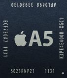
The Apple A5 chip, identified by the codename APL0498 and part number S5L8940, was a testament to advanced semiconductor manufacturing. Initially produced using a 45-nanometer fabrication process, later iterations benefited from a more refined 32nm High-K dielectric metal gate process. This miniaturization not only improved power efficiency but also allowed for a higher transistor density, though the exact transistor count for the A5 has not been publicly disclosed by Apple.
CPU Architecture and Performance:
The central processing unit (CPU) of the A5 featured two performance cores, capable of operating at clock speeds ranging from 800 MHz to 1 GHz. This dual-core configuration provided a substantial performance uplift compared to single-core processors, enabling more complex computations and a smoother user experience. Each performance core was equipped with a 32 KB L1 instruction cache (P-L1i) and a 32 KB L1 data cache (P-L1d), totaling 64 KB of L1 cache per core for rapid access to frequently used data and instructions. Furthermore, the A5 incorporated a 1 MB L2 cache shared by the performance cores, further accelerating data retrieval and processing.
A notable variant, the A5 chip found in the Apple TV (3rd generation), featured a single-core configuration. This strategic adaptation highlights Apple’s ability to tailor its silicon for specific product needs, optimizing for the unique requirements and power constraints of different devices. In this single-core variant, the L1 caches were reduced to 32 KB per core, reflecting a more focused performance profile.
Memory Subsystem:
The A5 chip’s memory subsystem was designed for high bandwidth and low power consumption, crucial for mobile devices. It utilized LPDDR2-800 memory, operating at a frequency of 400 MHz, and featured a 64-bit memory bus width. This configuration provided two memory channels, each 32 bits wide, resulting in a theoretical memory bandwidth of approximately 6.4 GB/s. The A5 chip was typically paired with 512 MB of RAM, a substantial amount for its time, which allowed for seamless multitasking and the execution of memory-intensive applications.
Graphics Processing Unit (GPU):
The graphical capabilities of the A5 were handled by an integrated GPU with two cores. This GPU was equipped with 4 SIMD (Single Instruction, Multiple Data) execution units and 32 FP32 (Floating-Point Single Precision) arithmetic logic units (ALUs). Operating at a clock speed of 200 MHz, the GPU was capable of delivering approximately 12.8 GFLOPS (Giga Floating-point Operations Per Second) of processing power. This provided the necessary horsepower for rendering smooth animations, displaying high-resolution graphics in games, and accelerating video playback, all of which were becoming increasingly important for mobile device users.

Timeline of the A5’s Impact
The introduction of the Apple A5 chip was not an isolated event but part of a carefully orchestrated product roadmap by Apple.
- March 11, 2011: The Apple A5 chip makes its debut, powering the iPad (2nd generation). This marked the first device to leverage the dual-core architecture and enhanced graphics of the A5.
- October 2011: The iPhone 4S is released, featuring a variant of the A5 chip (codenamed APL0498). This iteration was particularly significant as it brought advanced processing power and improved graphics to Apple’s flagship smartphone, enabling features like Siri and enhanced camera capabilities.
- March 2012: The iPad (3rd generation) also incorporates the A5 chip, offering a performance boost for Apple’s tablet lineup.
- March 2012: The Apple TV (3rd generation) is launched, utilizing a single-core version of the A5 chip (codenamed APL2498). This demonstrated Apple’s strategy of adapting its core silicon designs for specific product needs, optimizing for power efficiency and cost.
- Later Years: While newer Apple Silicon chips like the A6, A7, and subsequent generations quickly surpassed the A5 in performance and efficiency, the A5 remained in production and was integrated into various devices for an extended period, underscoring its robust design and cost-effectiveness for certain market segments.
Devices Powered by the Apple A5
The Apple A5 chip was a foundational component for a range of iconic Apple devices, contributing significantly to their success and user experience. Its versatility allowed it to be implemented across different form factors and functional requirements.
- iPad (2nd generation): The inaugural device to feature the A5, setting a new benchmark for tablet performance.
- iPhone 4S: The smartphone that introduced the A5 to a wider audience, enabling advanced features and a fluid user interface.
- iPad (3rd generation): Continued the legacy of the A5 in Apple’s tablet lineup, offering further performance enhancements.
- Apple TV (3rd generation): Utilized a specialized single-core variant of the A5, demonstrating Apple’s silicon customization capabilities.
- iPod Touch (5th generation): While often overlooked, the iPod Touch also benefited from the A5’s processing power, delivering a portable media and gaming experience.
Manufacturing and Supply Chain Considerations
The manufacturing of the Apple A5 chip by Samsung was a critical aspect of its production. At the time, Apple relied heavily on external foundries for its silicon fabrication. Samsung’s advanced manufacturing capabilities, particularly its prowess in 45nm and 32nm processes, made it a logical partner. However, this relationship was not without its complexities. As Apple’s own silicon designs grew more sophisticated and its market share expanded, the reliance on a competitor like Samsung became a strategic concern. This eventually led Apple to diversify its manufacturing partnerships and invest heavily in its own in-house chip design capabilities, aiming for greater control over its supply chain and intellectual property. The legal disputes that arose between Apple and Samsung in the following years, concerning patent infringements, further highlighted the intricate and often contentious nature of the semiconductor industry and the relationships between major technology players.

Analysis and Implications
The Apple A5 chip was more than just a component; it was a catalyst for innovation and a testament to Apple’s vertical integration strategy.
Performance Leap and User Experience
The dual-core architecture of the A5 represented a significant leap in mobile processing power. This translated directly into a smoother and more responsive user experience. Applications launched faster, multitasking became more fluid, and graphically intensive games and multimedia content could be rendered with greater fidelity. For the iPad (2nd generation), this meant a tablet that felt truly capable of productivity and entertainment, setting it apart from its competitors. In the iPhone 4S, the A5 powered the introduction of Siri, Apple’s groundbreaking voice assistant, which relied heavily on the chip’s processing power for natural language understanding and response generation.
Power Efficiency and Battery Life
A key challenge in mobile chip design is balancing performance with power consumption. The A5, especially with its move to the 32nm process, demonstrated Apple’s commitment to power efficiency. By optimizing its architecture and leveraging advanced fabrication techniques, Apple was able to deliver increased performance without a commensurate drain on battery life. This was crucial for devices that were expected to last a full day of use on a single charge. The ability to scale down clock speeds and power consumption for less demanding tasks, while ramping up for intensive operations, was a hallmark of the A5’s intelligent design.

Strategic Importance of In-House Silicon
The success of the A5 underscored the strategic importance of Apple’s in-house silicon design. By controlling the design process, Apple could precisely tailor its chips to the specific needs of its hardware and software ecosystem. This allowed for tighter integration between the chip and the operating system (iOS), leading to optimized performance and unique features that were difficult for competitors to replicate. The A5 was a crucial step in Apple’s journey towards developing its own powerful and efficient processors that would eventually redefine the personal computing landscape.
The A5’s Legacy and Future Impact
While the A5 has long been superseded by more advanced Apple Silicon chips, its legacy is undeniable. It laid the groundwork for the subsequent generations of A-series processors that would power iPhones, iPads, and eventually Macs. The A5 proved that Apple could not only design compelling hardware but also create the silicon that powered it, giving them a significant competitive advantage. Its dual-core architecture and focus on graphics and efficiency set a precedent for future mobile chip development across the industry. The A5 chip was a vital stepping stone, enabling Apple to push the boundaries of what was possible in mobile computing and cementing its reputation as an innovator in both hardware and software design. The ongoing evolution of Apple Silicon, from the A5 to the M-series chips found in modern Macs, is a direct continuation of the strategic vision that began with chips like the A5. This commitment to in-house silicon design continues to be a driving force behind Apple’s technological advancements and its ability to deliver highly integrated and performant user experiences.