Before Apple etched its own identity into the silicon landscape with the debut of the A4 chip in the iPhone 4, the company relied on Samsung for the crucial processors powering its nascent iOS devices. This era, marked by Samsung’s foundational role, set the stage for a monumental shift. Every iPhone, iPad, and iPod touch released since the original iPad has sported an Apple-designed System on a Chip (SoC), now famously known as the "A-Series," a nomenclature adopted from 2010 onwards. This strategic pivot transformed Apple from a hardware assembler into a vertically integrated technology powerhouse, controlling the very core of its device performance and innovation. The journey from these early Samsung-powered devices to the sophisticated, desktop-class A19 and A19 Pro chips found in the 2026 iPhone 17 lineup represents a remarkable testament to Apple’s relentless pursuit of performance, efficiency, and user experience.
The Genesis: Samsung’s Early Role and the A1 Chip
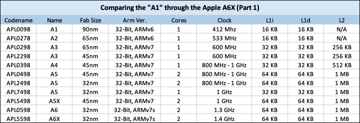
The story of Apple’s custom silicon begins not with Apple itself, but with its early reliance on external manufacturers. The first generation of the iPhone, iPod touch, and iPhone 3G were powered by chips identified as "APL0098" or, more technically, the Samsung S5L8900. This chip, part of the S5L89xx family, represented a departure from earlier prototypes that utilized Freescale i.MX31 processors. The decision to partner with Samsung for the S5L8900 was driven by a focus on power efficiency, a critical factor for the burgeoning mobile device market.
This early processor, also known by its ARM designation as the ARM 8900B, was a 32-bit ARMv6 core manufactured on a 90-nanometer process. Its clock speed was strategically limited to 412 MHz, a reduction from its default 666 MHz, further emphasizing its power-saving design. The chip featured a modest 16 KB of Level 1 Instruction cache and an equal amount for L1 data cache. Notably, it lacked any Level 2 or Level 3 cache, a stark contrast to modern SoCs. Its memory subsystem was equally basic, comprising 128 MB of LPDDR-266 RAM running at 133.25 MHz, providing a total memory bandwidth of 533 MB/s. This foundational chip, while rudimentary by today’s standards, was instrumental in bringing the iPhone and iPod touch to life, laying the groundwork for the mobile revolution.
The "A2" and the Dawn of the A3: Incremental Improvements
While Apple never officially branded a chip as the "A2," the processor found in the second-generation iPod touch serves as a logical successor to the A1. This chip, a variant of the S5L8900, was manufactured on a more advanced 65-nanometer process, signifying an early step towards greater efficiency and potential performance gains.
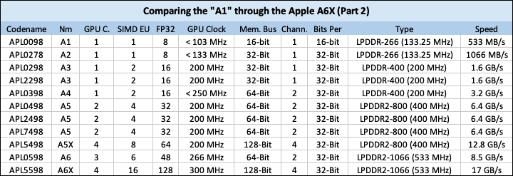
The true leap forward in this early era came with the "A3" series, encompassing the S5L8920 and S5L8922. The S5L8920 powered the iPhone 3GS, a device that marked a significant performance upgrade over its predecessors. Its variant, the S5L8922, found its way into the third-generation iPod touch. The A3 series distinguished itself from the A1/A2 by doubling the L1 Instruction and data caches to 32 KB per core. This enhancement, coupled with an increase in memory bandwidth to 1.6 GB/s, facilitated by 256 MB of LPDDR-400 RAM running at 200 MHz, contributed to a noticeable performance boost. A significant architectural addition was the introduction of a 256 KB L2 cache, a feature conspicuously absent in earlier iOS devices, which greatly improved the chip’s ability to handle more complex tasks and access frequently used data. The GPU clock speed also saw an increase to 200 MHz, further enhancing graphical capabilities.
The A4: Apple’s First In-House Design and the Dawn of a New Era
The year 2010 marked a pivotal moment in Apple’s technological trajectory with the introduction of the A4 chip. This was the first Apple-designed SoC, built in-house, signaling Apple’s strategic commitment to controlling its hardware destiny. The A4 powered iconic devices such as the iPhone 4, the original iPad, and the fourth-generation iPod touch.
While still a 32-bit processor, the A4 represented a substantial upgrade. It featured a larger 512 KB L2 cache, a doubling of the previous generation’s capacity. CPU clock speeds were also incrementally increased, ranging from 800 MHz to 1 GHz depending on the device. Memory bandwidth saw a significant jump to 3.2 GB/s, demonstrating Apple’s focus on accelerating data flow within the chip. This marked a clear departure from the outsourced, power-efficiency-focused approach of its early days, establishing a new benchmark for mobile performance and setting the stage for the highly integrated Apple Silicon we know today.

The A5 and A5X: Dual-Core Power and Enhanced Graphics
The A5 chip, introduced in March 2011 with the second-generation iPad, was a significant step towards multi-core processing. Apple touted its "dual-core" capabilities, claiming it could "do twice the work" of the A4 and deliver nine times the graphical performance. The A5 featured an improved L2 cache, faster memory, and a more capable graphics core. All A5 and A5X chips incorporated 1 MB of L2 cache.
A notable exception within the A5 family was a locked-down, single-core version specifically designed for the third-generation Apple TV. This demonstrated Apple’s increasing ability to tailor its silicon for specific product needs and optimize for different power envelopes.
The A5X, launched with the third-generation iPad, was a higher-performance variant designed to handle more demanding graphical tasks. It featured a quad-core graphics chip, pushing graphical performance to an impressive 25.6 Gigaflops. This variant showcased Apple’s ambition to equip its tablets with graphics capabilities that rivaled entry-level PCs, enabling richer media experiences and more complex applications.
The A6 and A6X: Pushing Clock Speeds and Memory Bandwidth
The A6 and A6X chips represented further advancements in raw processing power and memory architecture. The A6, powering the iPhone 5 and 5c, achieved CPU clock speeds of 1.3 GHz. The A6X, featured in the fourth-generation iPad, pushed this further to 1.4 GHz.
A key upgrade in the A6 series was the adoption of LPDDR2-1066 RAM, operating at 533 MHz. This resulted in a memory bandwidth of 8.5 GB/s for iPhones and a remarkable 17 GB/s for the fourth-generation iPad. The GPU clock speeds also saw a boost, with the A6 variants operating at 266 MHz and the A6X at 300 MHz. These improvements were crucial for handling increasingly sophisticated mobile applications, high-definition video playback, and more demanding gaming experiences.
The A7: The 64-Bit Revolution in Mobile
September 10th, 2013, marked another watershed moment with the introduction of the A7 chip alongside the iPhone 5s. This was the world’s first 64-bit mobile SoC, a groundbreaking achievement that significantly expanded the potential for mobile computing. The A7 was also used in the second and third generations of the iPad mini, as well as the original iPad Air.
Featuring an estimated one billion transistors and manufactured on an even smaller fabrication process, the A7 delivered substantial improvements. Its 64-bit architecture allowed for a larger addressable memory space and more efficient instruction processing, paving the way for more powerful and complex software. The transition to 64-bit was a strategic move that aligned Apple’s mobile silicon with its desktop and server architectures, promising seamless integration and greater performance ceilings.
The A8 and the Popularity of Larger iPhones
The release of the iPhone 6 and 6 Plus in 2014 coincided with the A8 chip, a processor that powered what would become Apple’s most popular iPhones ever. With approximately a quarter of a billion devices sold worldwide, these models were not only the most popular iPhones but also the most popular smartphones to date. The A8 chip, while not as revolutionary as the A7 in terms of architectural shifts, continued Apple’s trend of delivering robust performance and efficiency, perfectly complementing the larger displays and enhanced user experiences of these flagship devices.
The A9, A9X, and the Rise of TSMC
The A9 and A9X chips, introduced with the iPhone 6s and 6s Plus, saw a significant change in manufacturing. While an initial version of the A9 was produced by Samsung, Apple also partnered with TSMC (Taiwan Semiconductor Manufacturing Company) for a later version, utilizing a more advanced manufacturing process. This diversification of manufacturing partners was a strategic move to ensure supply chain stability and leverage the strengths of different foundries.
The A9 series was also notable for being the first Apple devices to utilize DDR4 memory, predating its adoption in Macs by approximately two years. This provided a significant boost in memory performance. Furthermore, the A9 chip introduced a custom Apple-designed NVMe controller, incorporating PCI Express technology. This custom storage solution dramatically increased internal storage speeds on iPhones, a critical improvement for handling larger app sizes, higher-resolution photos, and 4K video recording. This marked a significant step in optimizing the entire system, not just the processor.
The A10 Fusion, A10X Fusion, and the T2 Chip: Efficiency and Integrated Security
The iPhone 7 and 7 Plus, released in September 2016, featured the A10 Fusion, a chip that ushered in a new era of power efficiency. The A10 Fusion was Apple’s first quad-core SoC, but it differentiated itself by employing a "big.LITTLE" architecture, featuring two high-performance cores and two high-efficiency cores. This allowed the chip to intelligently switch between cores based on workload, optimizing battery life without sacrificing performance. Apple claimed the A10 Fusion offered 40% better CPU performance and 50% more GPU performance than its predecessor, the A9.
Alongside the A10 Fusion, Apple also introduced the A10X Fusion for its third-generation iPad Pro, further pushing graphical and computational capabilities. This chip was designed to handle the most demanding professional workloads on a tablet.
The introduction of the T2 chip, while not part of the A-series, is a crucial element in Apple’s silicon strategy. The T2 chip acts as a secure enclave processor, integrating various controllers for storage, audio, and secure boot, enhancing the overall security and functionality of Mac computers. Its presence signifies Apple’s commitment to building highly integrated and secure systems.
The A11 Bionic: Neural Engine and the Shift to Neural Processing
The A11 Bionic, launched with the iPhone 8, 8 Plus, and iPhone X, was a significant leap forward, most notably for its integrated Neural Engine. This dedicated hardware accelerator was designed to perform machine learning tasks at an unprecedented speed and efficiency. The Neural Engine enabled features like facial recognition (Face ID), advanced computational photography, and more sophisticated AI-driven applications. The A11 was a true testament to Apple’s foresight in embracing the age of artificial intelligence and machine learning, embedding these capabilities directly into the core of its devices.
The A12 Bionic and A12X Bionic: Efficiency and Enhanced Neural Capabilities
The A12 Bionic, found in the iPhone XS, XS Max, and XR, continued to refine the architecture introduced with the A11. Manufactured on a more advanced 7-nanometer process, it offered improved performance and power efficiency. The Neural Engine was further enhanced, capable of performing up to five trillion operations per second, enabling even more sophisticated AI features.
The A12X Bionic, powering the third-generation iPad Pro, represented a significant step up in raw power, effectively blurring the lines between mobile and desktop computing. Its enhanced Neural Engine and robust CPU and GPU performance made it capable of handling professional-grade tasks such as video editing and 3D rendering.
The A13 Bionic: Performance and Power Efficiency Pinnacle
The A13 Bionic, powering the iPhone 11 series, represented a new pinnacle in performance and power efficiency. Manufactured on a 7-nanometer process, it delivered significant gains in CPU and GPU speeds while further optimizing power consumption. The Neural Engine was once again improved, becoming even faster and more capable, solidifying Apple’s commitment to machine learning. This chip showcased Apple’s mastery of silicon design, achieving an impressive balance of raw power and battery longevity.
The A14 Bionic and the Dawn of 5nm
The A14 Bionic, introduced with the fourth-generation iPad Air and later the iPhone 12 series, marked Apple’s transition to a 5-nanometer manufacturing process. This smaller process node allowed for even greater transistor density, leading to substantial improvements in performance and efficiency. The A14 Bionic delivered industry-leading performance, enabling advanced features like Dolby Vision HDR recording and powering the increasingly complex demands of 5G connectivity.

The A15 Bionic and the iPhone 13 Series
The A15 Bionic, featured in the iPhone 13 lineup, continued to refine the 5nm process and delivered further performance and efficiency gains. It offered improved CPU and GPU performance, a more advanced Neural Engine for enhanced AI capabilities, and optimized power management for longer battery life. The A15 Bionic showcased Apple’s iterative but impactful approach to silicon development, consistently pushing the boundaries of what’s possible in mobile computing.
The A16 Bionic: Dynamic Island and Further Refinements
The A16 Bionic, introduced with the iPhone 14 Pro and iPhone 14 Pro Max, represented another step in Apple’s silicon evolution. While still based on a 4nm process (an enhancement of the 5nm node), it delivered improved performance and efficiency. A key innovation tied to the A16 Bionic was the introduction of the "Dynamic Island," an interactive and fluid area that replaced the notch, showcasing Apple’s ability to integrate hardware and software for novel user experiences. The Neural Engine also saw further enhancements, improving the capabilities of machine learning-driven features.
The Future: A17 and Beyond – Desktop-Class Performance
Looking ahead to 2026, the iPhone 17 lineup is expected to feature the A19 and A19 Pro chips. These future iterations are anticipated to deliver true desktop-class multicore processing, unparalleled graphical power, and responsiveness, further blurring the lines between smartphones, tablets, and traditional computers. The trajectory from the early Samsung S5L8900 to these advanced future chips highlights an incredible journey of innovation, strategic foresight, and an unwavering commitment to pushing the boundaries of mobile technology. Apple’s control over its silicon design and manufacturing has not only defined its own product ecosystem but has also profoundly shaped the entire mobile industry, setting a benchmark for performance, efficiency, and integrated user experiences.