Before Apple revolutionized personal computing with its custom in-house silicon, the initial wave of iOS devices relied on chips from Samsung. These early System on a Chip (SoC) designs laid the groundwork for the company’s future success, with every iPad and subsequent iPhone featuring Apple-designed processors since the introduction of the A4 chip. This lineage of processors, known as the "A-Series," has seen remarkable advancements, transforming smartphones and tablets into devices capable of desktop-class performance. By 2026, the iPhone 17 lineup is expected to showcase the A19 and A19 Pro chips, boasting multicore processing power, graphical capabilities, and responsiveness that rival traditional desktop computers. This journey, marked by incremental yet significant improvements, highlights Apple’s strategic commitment to vertical integration and its unwavering pursuit of silicon innovation.
The Genesis: Samsung’s Role in Early iOS Devices
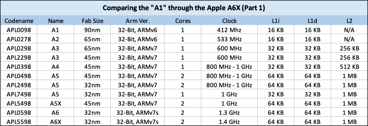
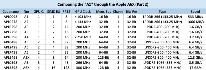
The story of Apple’s custom silicon begins not with an Apple design, but with a partnership. The very first iOS devices, including the original iPhone, the first-generation iPod touch, and the iPhone 3G, were powered by chips manufactured by Samsung. These early processors, often identified by internal codenames like "APL0098" and later more broadly by Samsung’s S5L89xx series, were crucial for establishing the foundational capabilities of these groundbreaking devices.
The "APL0098," also known as the Samsung S5L8900, was a 32-bit ARMv6 processor. While it operated at an underclocked 412 MHz from its default 666 MHz, it was designed with a focus on power efficiency rather than raw performance. Its architecture included a modest 16 KB of L1 instruction cache and another 16 KB for L1 data cache. Notably, it lacked any L2 or L3 cache, relying on a single processor core. Memory was handled by 128 MB of 133.25 MHz LPDDR-266 RAM, providing a memory bandwidth of approximately 533 MB/s. This configuration was a significant departure from the high-performance processors found in contemporary computers, but it was precisely what was needed to enable the novel functionalities of the early iPhone and iPod touch.
Following the S5L8900, the second-generation iPod touch incorporated a chip that, while not officially branded "Apple A2," served as its successor. This chip, a 65nm variant, offered minor improvements over its predecessor, continuing the trend of prioritizing efficiency.
The Leap to the A3: Enhanced Performance and Memory
A significant step forward arrived with the chips designated as S5L8920 and S5L8922, often colloquially referred to as the "Apple A3." The S5L8920 powered the iPhone 3GS, while the S5L8922 found its way into the third-generation iPod touch. These chips marked a notable improvement by doubling the L1 instruction and data caches to 32 KB per core, contributing directly to enhanced performance.
Furthermore, memory bandwidth saw a substantial increase, doubling to 1.6 GB/s. This was achieved through 256 MB of LPDDR-400 (200 MHz) RAM, offering greater capacity and speed. The graphics processing unit (GPU) also received a boost, with its clock speed increasing to 200 MHz. Crucially, this generation of chips introduced the long-awaited 256 KB of L2 cache, a feature that had been absent in previous iOS devices and was instrumental in smoothing out performance and improving multitasking capabilities.
The Dawn of In-House Design: The A4 Chip
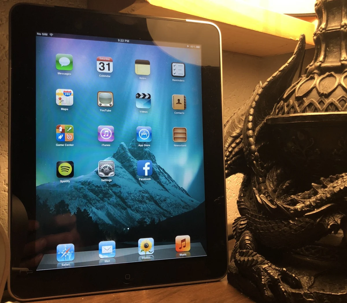
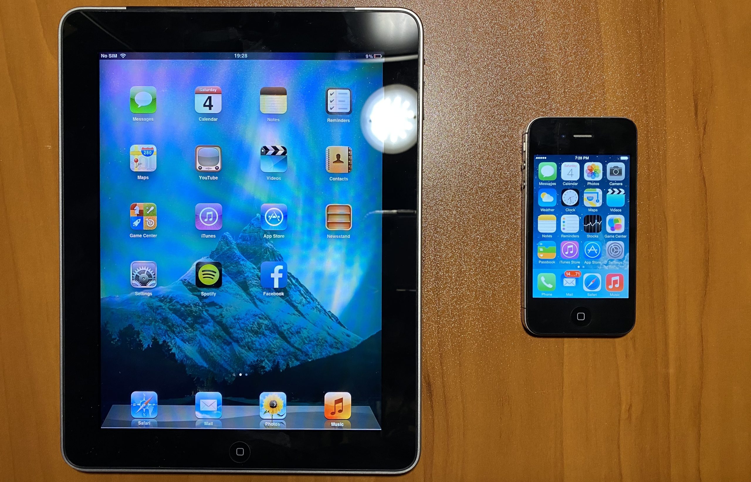
The year 2010 marked a pivotal moment in Apple’s history with the introduction of the A4 chip. This was Apple’s first custom-designed SoC, signaling a strategic shift towards in-house silicon development. The A4 powered devices such as the iPhone 4, the original iPad, and the fourth-generation iPod touch.
While still a 32-bit processor, the A4 represented a considerable leap in performance. It featured a 512 KB L2 cache, a doubling of the previous generation’s capacity. CPU clock speeds were also incrementally increased, ranging from 800 MHz to 1 GHz, depending on the device. Memory bandwidth saw another significant jump to 3.2 GB/s across all devices utilizing this SoC. This move towards custom silicon allowed Apple greater control over performance, power efficiency, and the integration of features tailored to its software ecosystem.
Iterative Power: The A5 and A5X Series
The A5 chip, released in March 2011 with the second-generation iPad, was a substantial upgrade over the A4. Apple promoted it as capable of "twice the work" and boasting nine times the graphical performance. The A5 featured improved L2 cache, faster memory, and an enhanced graphics core. All A5 and A5X chips incorporated 1 MB of L2 cache.
A notable aspect of the A5 generation was the existence of multiple variants. While commonly associated with dual-core configurations, a locked-down single-core version was developed specifically for the third-generation Apple TV. This demonstrated Apple’s ability to tailor its silicon designs for specific product needs and thermal envelopes.
The A5X, introduced with the third-generation iPad, was a higher-performance iteration of the A5. It featured a quad-core graphics chip, pushing graphical performance to approximately 25.6 Gigaflops and incorporating several technical refinements over the standard A5. This dual-track approach—offering both general-purpose and graphics-intensive variants—allowed Apple to optimize performance across a wider range of applications and device categories.
Pushing Boundaries: The A6 and A6X
The A6 and A6X chips represented further advancements, with CPU clock speeds finally surpassing the 1 GHz threshold. The iPhone 5 and 5c were powered by chips clocked at 1.3 GHz, while the fourth-generation iPad featured the A6X at 1.4 GHz. The memory subsystem also saw upgrades, with the A5 series transitioning to LPDDR2-1066 (533 MHz) RAM, providing a memory bandwidth of 8.5 GB/s for iPhones and a remarkable 17 GB/s for the fourth-generation iPad. The GPU clock speeds also saw a modest increase, with the iPhone 5/5c at 266 MHz and the fourth-generation iPad’s A6X at 300 MHz. These incremental improvements continued to enhance the responsiveness and graphical fidelity of Apple’s devices.
A Paradigm Shift: The 64-Bit A7 Chip
September 10th, 2013, marked a revolutionary moment with the introduction of the Apple A7 chip. This processor was the first mobile chip to feature a 64-bit architecture, a significant leap that would redefine mobile computing. The A7 powered devices including the iPhone 5s, the second and third-generation iPad mini, and the original iPad Air.
Boasting one billion transistors and an even smaller fabrication process, the A7 delivered substantial improvements over its predecessors. The transition to 64-bit allowed for larger memory address spaces, improved performance for demanding applications, and better energy efficiency. This architectural shift laid the foundation for the increasingly complex and powerful mobile experiences that would follow.
The Popularity of the iPhone 6 and the A8 Chip
The iPhone 6 and 6 Plus, released alongside the A8 chip, became Apple’s most popular iPhones to date, selling approximately a quarter of a billion units worldwide. This immense popularity underscored the market’s demand for larger screen devices and highlighted the A8’s role in delivering a smooth and capable user experience. While specific technical details of the A8 are less publicly detailed compared to some other generations, it continued the trajectory of performance and efficiency improvements, ensuring these widely adopted devices met consumer expectations.
A New Manufacturer and Storage Innovation: A9 and A9X
The A9 and A9X generation introduced a significant change in manufacturing. While some A9 chips were produced by Samsung, Apple also began a crucial partnership with TSMC (Taiwan Semiconductor Manufacturing Company) for its silicon production. This diversification of manufacturing was a strategic move to ensure supply chain resilience and leverage the advanced manufacturing capabilities of different foundries.
The A9 chip also marked a significant advancement in storage technology. It incorporated an Apple-designed NVMe controller, leveraging the PCI Express interface. This resulted in substantially faster internal storage speeds for the iPhone 6s and subsequent models, a crucial development as apps and media files grew in size and complexity. This innovation in storage architecture predated similar advancements in Macs by several years, showcasing Apple’s commitment to optimizing the entire system. Furthermore, the A9 was among the first Apple devices to utilize DDR4 RAM, outperforming Macs by approximately two years in adopting this faster memory standard.
Efficiency and Power: The A10 Fusion and A10X Fusion
The release of the iPhone 7 and 7 Plus on September 16th, 2016, brought the A10 Fusion chip, a groundbreaking SoC that introduced the concept of "efficiency cores" to Apple’s mobile lineup. The A10 Fusion was Apple’s first quad-core mobile SoC, featuring two high-performance cores and two high-efficiency cores. This hybrid architecture allowed the chip to dynamically allocate tasks, prioritizing performance when needed and conserving power during less demanding operations. According to Apple’s announcements, the A10 Fusion offered 40% better CPU performance and 50% more GPU performance compared to the A9.
The A10X Fusion, featured in the third-generation iPad Pro, represented an even more powerful iteration, likely incorporating more cores and higher clock speeds to handle the demanding workloads of a tablet. The introduction of efficiency cores was a pivotal moment, setting a precedent for power management strategies in future mobile processors across the industry.
The T2 Chip: Security and System Management
Alongside the advancements in A-series processors, Apple also introduced the T2 chip, a dedicated security and system management controller. Initially appearing in Macs, the T2 chip integrated various controllers, including the system management controller, image signal processor, audio controller, and SSD controller. Most importantly, it housed the Secure Enclave, providing hardware-level security for data encryption and biometric authentication. While not directly an A-series chip for consumer devices like iPhones and iPads, its development highlighted Apple’s expanding ambition in custom silicon design, extending into critical areas like security and system integration.
The Continuous Pursuit of Performance and Efficiency
The progression from Samsung-manufactured chips to Apple’s highly integrated A-series processors is a testament to the company’s long-term vision and relentless pursuit of technological excellence. Each generation has built upon the innovations of its predecessor, introducing architectural advancements, faster memory technologies, more sophisticated graphics, and improved power management. The journey from the modest capabilities of the "APL0098" to the projected desktop-class performance of the A19 and A19 Pro by 2026 underscores Apple’s commitment to controlling its hardware destiny and delivering a seamless, powerful, and efficient user experience across its diverse product ecosystem. This strategic focus on in-house silicon design has not only driven Apple’s success but has also profoundly influenced the trajectory of the entire mobile and personal computing industries.