 Vera Clarissa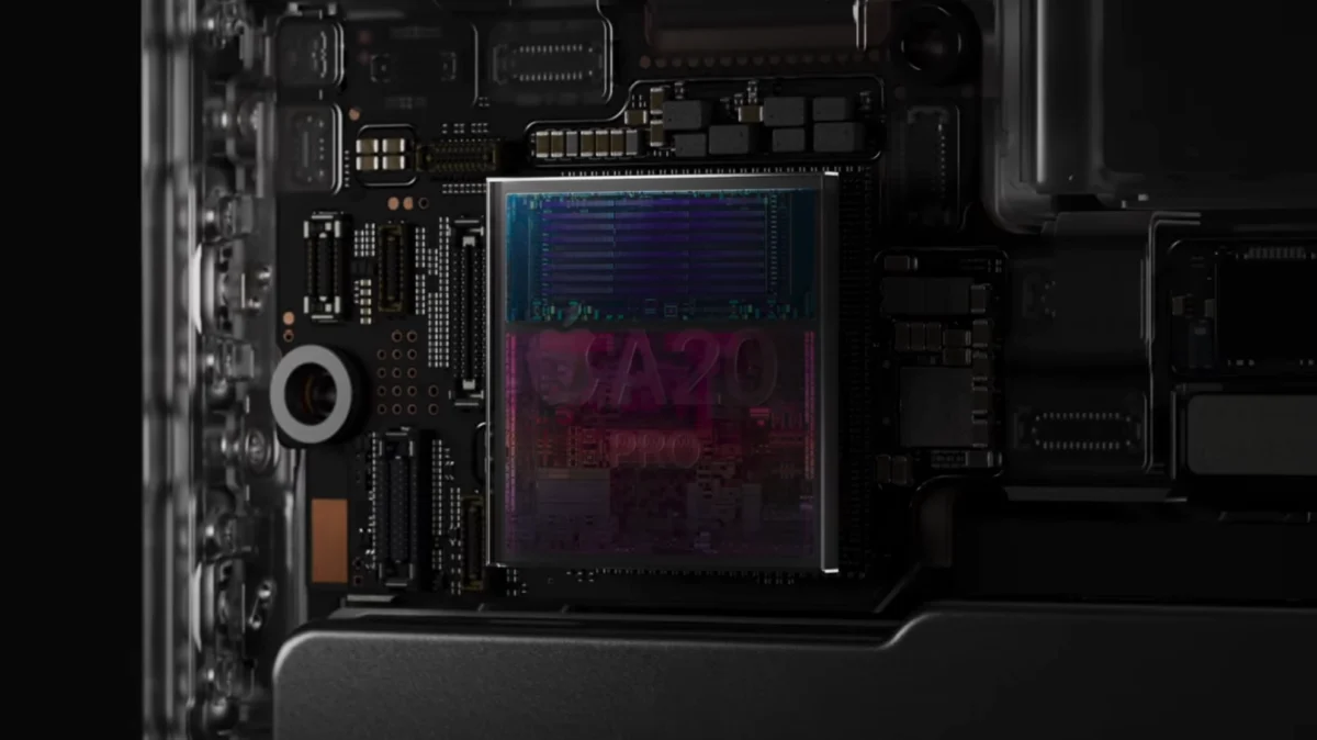
The average width of a human hair spans approximately 50 to 120 micrometers, or between three and five thousandths of an inch. When one takes 0.005 inches and divides it by 63,500, the resulting figure is 2 nanometers—the physical scale of the transistor architecture powering the A20 Pro chip. Integrated into the new iPhone 18 Pro and iPhone 18 Pro Max, this silicon represents a significant leap in semiconductor density and efficiency, marking the latest milestone in Apple’s decade-long transition toward fully custom-designed, high-performance mobile computing.
Architectural Evolution: The Shift to 2nm
The A20 Pro is not merely a refinement of previous mobile silicon; it is a fundamental architectural overhaul. Drawing inspiration from the M-series chips that revolutionized the MacBook lineup, the A20 Pro adopts a design where memory modules are positioned directly alongside the main silicon die. This spatial configuration, often referred to as a unified or adjacent memory architecture, serves a primary functional goal: superior thermal management. By placing memory in close proximity to the processor, engineers have facilitated a more efficient path for heat dissipation into the device’s integrated vapor chamber.

This hardware redesign is accompanied by a substantial increase in memory bandwidth, which has been elevated by 50% to 113.7 GB/s. For the end user, this translates to faster data throughput, enabling the device to handle complex computational tasks—such as high-fidelity neural processing and real-time ray tracing—with significantly less latency.
Chronology of Silicon Advancement
To understand the significance of the A20 Pro, one must view it within the broader timeline of Apple Silicon development. In 2020, Apple introduced the M1 chip, which effectively erased the performance gap between mobile-derived architectures and traditional desktop-class hardware. Since then, the trajectory has been one of consistent, iterative growth.
- 2020: The M1 chip debuts, setting a new benchmark for power efficiency in the laptop sector.
- 2021–2023: The A-series chips move from 5nm to 3nm processes, focusing on core count increases and power efficiency.
- 2024: The M4 architecture pushes the boundaries of thermal efficiency in the portable Mac category.
- 2026: The A20 Pro arrives, utilizing a 2nm fabrication process to pack unprecedented density into the iPhone 18 Pro.
This progression demonstrates that Apple’s strategy has shifted from simply increasing raw clock speeds to optimizing the entire system-on-chip (SoC) environment. By moving the memory closer to the logic, Apple is addressing the "bottleneck" problem that has long plagued high-performance mobile devices.

Benchmarking Performance: A20 Pro vs. The Field
Geekbench 6.7.x data reveals a performance profile that challenges the traditional hierarchy between mobile and desktop computing. When compared against the M1 MacBook Air, the A20 Pro demonstrates more than double the single-core CPU and Metal GPU performance. Even more notable is the comparison to the M4 MacBook Air; the A20 Pro manages to nearly match the M4 in multi-core CPU performance, a feat that would have been considered impossible for a smartphone chip just three years ago.
The A20 Pro achieves a peak clock speed of 4.93 GHz, a notable jump from the 4.26 GHz found in the A19 Pro. This performance increase is bolstered by an expanded cache hierarchy. Apple has intentionally increased the L1 instruction cache, L1 data cache, and L2 cache, ensuring that the processor spends less time waiting for data from the main memory and more time executing instructions.
Comparative Data Analysis
| Chipset | Architecture | Clock Speed | Memory Bandwidth |
|---|---|---|---|
| M1 | 5nm | ~3.2 GHz | 68.25 GB/s |
| A19 Pro | 3nm | 4.26 GHz | ~75 GB/s |
| A20 Pro | 2nm | 4.93 GHz | 113.7 GB/s |
These figures suggest that the A20 Pro is essentially a desktop-grade processor disguised as a mobile chip. While benchmarks are synthetic—functioning as a "water pressure test" to see how much strain a system can withstand under controlled conditions—the delta between the A20 Pro and its predecessors is wide enough to suggest that the real-world experience for power users will be substantially different.

Industry Reactions and Expert Perspectives
While Apple has remained characteristically sparse on technical minutiae during public events, industry analysts have been quick to note the implications of the 2nm move. Semiconductor analysts suggest that the jump to 2nm is not just about raw power, but about maintaining performance while keeping thermal envelopes manageable.
"The move to 2nm allows Apple to keep the power draw low while increasing the transistor count," says an industry consultant familiar with foundry roadmaps. "By moving the memory, they are essentially creating a ‘mini-M-series’ chip for the iPhone. This is not just an upgrade to the CPU; it is a total redesign of the computational environment of the phone."
Broader Implications for Mobile Computing
The implications of the A20 Pro are twofold: one for the consumer market and one for the software development ecosystem. For consumers, the device promises a longer "useful life." As software becomes increasingly bloated with AI-driven features and real-time processing requirements, the A20 Pro’s headroom ensures the hardware will remain relevant for several years.

For developers, the performance ceiling of the A20 Pro encourages the creation of applications that were previously reserved for high-end workstations. We are likely to see more robust, desktop-class creative suites—such as professional video editing, 3D rendering, and local large-language model (LLM) execution—moving from the Mac to the iPhone.
Furthermore, the integration of 2nm technology signals a potential slowdown in the traditional "Moore’s Law" curve, as physical limitations begin to play a larger role. However, by optimizing memory proximity and cache sizes, Apple is proving that performance gains can still be eked out through architectural intelligence even when manufacturing nodes reach their physical limits.
The Sustainability of High-Performance Silicon
An often-overlooked aspect of this leap is power efficiency. In a standard computational model, increasing clock speed typically results in exponential increases in power consumption and heat. By utilizing the 2nm node, Apple can achieve these 4.93 GHz speeds at a power envelope that is comparable to, or even lower than, previous generations. This is critical for the iPhone, where battery capacity is inherently limited by the physical constraints of the chassis.

As the smartphone market matures, the differentiation between "Pro" and "non-Pro" models is increasingly defined by the silicon. The A20 Pro, with its bespoke memory placement and advanced cache architecture, reinforces the iPhone 18 Pro’s position as a serious professional tool rather than just a communication device.
In conclusion, the A20 Pro stands as a testament to the maturation of Apple Silicon. By bridging the gap between mobile and desktop-class architectures, Apple has effectively created a new category of portable power. Whether this will lead to a full convergence of iOS and macOS remains a subject of intense industry speculation, but for now, the A20 Pro provides the hardware foundation necessary to make such a future a technical possibility. The focus now turns to how software developers will leverage this massive increase in bandwidth and processing headroom in the coming months.