Before the advent of Apple’s proprietary in-house silicon, marked by the debut of the A4 chip in the iPhone 4, early iOS devices relied on processors manufactured by Samsung. This foundational period saw Samsung chips powering the initial iterations of Apple’s groundbreaking mobile devices. However, with the release of the first iPad, Apple embarked on a new trajectory, designing and implementing its own custom System on a Chip (SoC) solutions, which would come to be known as the "A-Series" chips, a naming convention firmly established from 2010 onwards. Fast forward to the present day, and the iPhone 17 lineup, released in 2026, showcases the culmination of this decades-long innovation: the A19 and A19 Pro chips. These processors deliver unprecedented desktop-class multicore processing, formidable graphical capabilities, and a level of responsiveness that blurs the lines between smartphones, tablets, and traditional computing devices. While current mobile Apple SoCs now rival established chips like the M1, the journey has been one of meticulous, incremental progress, with each generation building upon the successes and lessons learned from its predecessors.
The Genesis: Early Samsung-Powered Devices
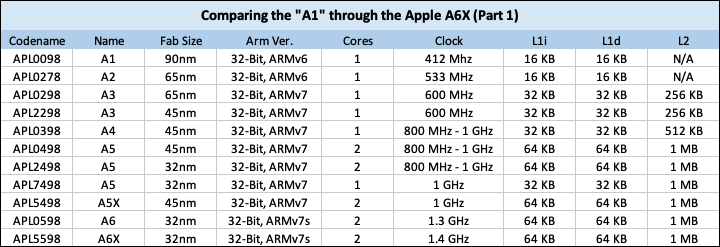
The earliest chapter in Apple’s mobile chip history is intrinsically linked to Samsung. The very first iPhone, iPod touch, and the iPhone 3G were powered by chips designated as "APL0098," more commonly known by their Samsung S5L8900 designation. These S5L89xx series chips were adopted after initial iPhone prototypes utilized Freescale i.MX31 processors. The design philosophy for these early Samsung-sourced chips prioritized power efficiency over raw performance, a crucial consideration for the nascent smartphone market where battery life was a paramount concern.
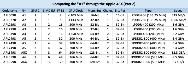
The "APL0098" or Samsung S5L8900, also recognized as the ARM 8900B, was a 32-bit ARMv6 processor manufactured on a 90-nanometer process. Its clock speed was deliberately underclocked to 412 MHz from a default of 666 MHz, further emphasizing power conservation. Cache configuration was rudimentary by today’s standards, featuring 16 KB of Level 1 Instruction cache and an equivalent 16 KB for L1 data cache. Notably, there was no L2 or L3 cache, and no shared system cache. The single processor core was paired with 128 MB of LPDDR-266 RAM operating at 133.25 MHz, providing a total memory bandwidth of 533 MB/s.
A closely related chip, often colloquially referred to as the "Apple A2," was utilized exclusively in the second-generation iPod touch. While not officially branded as an "A2," this designation is fitting given its sequential role. This processor was a refinement of the A1’s architecture, manufactured on a more advanced 65nm process. While sharing many similarities with the S5L8900, it incorporated other subtle differences, reflecting ongoing optimization efforts.
The Dawn of In-House Design: The A4 Chip and Beyond
The landscape of Apple’s mobile processors underwent a significant transformation with the introduction of the A4 chip. This marked Apple’s definitive entry into in-house SoC design, mirroring the strategy that would later define its highly successful Apple Silicon M-series chips for Macs. The A4 powered the iPhone 4, the original iPad, and the fourth-generation iPod touch. It represented a substantial leap forward in performance and architecture.
The A4 chip, still a 32-bit design, featured a doubled L2 cache size compared to its predecessors, increasing to 512 KB. CPU clock speeds saw an incremental boost, reaching up to 800 MHz and even 1 GHz in certain devices. Memory bandwidth also increased to 3.2 GB/s across all devices equipped with this SoC. This was a critical step in Apple’s journey to control its hardware destiny, allowing for deeper integration of hardware and software and greater optimization for its specific product ecosystem.
The A5 Era: Dual-Core Power and Enhanced Graphics
The A5 chip, introduced in March 2011 alongside the second-generation iPad, ushered in the era of dual-core processing for Apple’s mobile devices. Apple marketed the A5 as capable of "doing twice the work" of the A4, with a ninefold increase in graphical performance. All A5 and A5X chips featured an improved 1 MB L2 cache, faster memory, and a more potent graphics core.

Interestingly, the A5 family included variations. A locked-down single-core version was specifically developed for the third-generation Apple TV, showcasing Apple’s ability to tailor processor configurations for different product needs. The A5X, featured in the third-generation iPad, represented a significant enhancement. It incorporated a quad-core graphics chip, boosting graphical performance to an impressive 25.6 Gigaflops and introducing a host of technical improvements over the standard A5.
The A6 and A6X: Pushing Clock Speed Boundaries
The A6 and A6X chips marked another significant milestone, with CPU clock speeds finally surpassing the 1 GHz threshold. The iPhone 5 and 5c were equipped with chips running at 1.3 GHz, while the fourth-generation iPad utilized the A6X at 1.4 GHz. The RAM architecture also saw an upgrade to LPDDR2-1066, providing a memory bandwidth of 8.5 GB/s for the iPhone models and an even more substantial 17 GB/s for the fourth-generation iPad. The GPU clock speeds also saw an increase, reaching 300 MHz on the iPad 4th-gen compared to 266 MHz on the iPhone 5/5c.
The A7: A 64-Bit Revolution in Mobile Computing
A pivotal moment in mobile processor history arrived with the introduction of the Apple A7 chip on September 10, 2013, alongside the iPhone 5s. This chip was not only a performance powerhouse but also the first 64-bit mobile Apple Silicon ever created. The A7 also found its way into the second and third generations of the iPad mini, as well as the original iPad Air.
Featuring an estimated one billion transistors and manufactured on an even smaller process node, the A7 delivered a significant array of improvements over its predecessors. The move to a 64-bit architecture was a groundbreaking shift, enabling devices to address more memory and execute more complex instructions, laying the groundwork for the sophisticated applications and operating systems of the future. This architectural leap was a testament to Apple’s foresight in anticipating the evolving demands of mobile computing.
The iPhone 6 Era: Popularity and the A8 Chip
The release of the iPhone 6 and 6 Plus in 2014 coincided with the introduction of the Apple A8 chip. These devices became incredibly popular, with the iPhone 6 and 6 Plus selling an estimated quarter of a billion units worldwide, making them the most popular iPhones ever released and, at the time, the most popular smartphones globally. This widespread adoption underscored the growing reliance on powerful and efficient mobile processors.
The A8 chip, while not as architecturally revolutionary as the A7, represented a solid iterative improvement, further enhancing performance and efficiency for the flagship iPhones. The success of these models directly fueled the demand for more advanced processing capabilities in subsequent generations.
The A9 and A9X: Shifting Manufacturing and Advanced Storage
The A9 and A9X chips, introduced with the iPhone 6s and 6s Plus, marked another significant shift. For the first time, Apple utilized TSMC as a manufacturing partner alongside Samsung for the A9 chip. One version of the A9 was produced by Samsung, powering the 6s and 6s Plus, while a nearly identical TSMC version was used in the iPhone SE. This dual-sourcing strategy likely aimed to ensure supply chain robustness and potentially leverage competitive pricing.
A key technological advancement with the A9 was its adoption of DDR4 RAM, predating its implementation in Macs by approximately two years, with DDR4 not appearing in iMacs until 2017. Furthermore, the A9 chip featured a brand-new, custom-designed NVMe controller developed by Apple. This integrated an NVMe interface, enabling PCI Express connectivity and dramatically faster internal storage for the iPhone 6s and subsequent models. This development was instrumental in the rapid evolution of mobile storage speeds, paving the way for richer media experiences and faster app loading times.
The A10 Fusion and A10X Fusion: The Dawn of Efficiency Cores
September 16, 2016, saw the release of the iPhone 7 and 7 Plus, powered by the A10 Fusion chip. This introduction was monumental as it brought forth the concept of "Efficiency Cores" to Apple’s mobile SoCs, a design principle that has become a cornerstone of modern processor architecture. The A10 Fusion was Apple’s first quad-core SoC, boasting a claimed 40% improvement in CPU performance and a 50% increase in GPU performance over the A9, according to Apple’s official statements. The integration of high-performance cores for demanding tasks and high-efficiency cores for background processes and lighter workloads represented a significant stride in power management and overall device responsiveness.
The A10X Fusion chip, found in devices like the 10.5-inch and 12.9-inch iPad Pro (2nd generation), further pushed the boundaries of mobile processing. It featured an enhanced CPU with more high-performance cores and an even more powerful GPU, delivering desktop-caliber performance for demanding professional applications on a tablet form factor.
The T2 Chip: A Specialized Security and Control Hub
While not part of the main A-series lineage for iPhones and iPads, the T2 chip warrants mention in the broader context of Apple’s custom silicon development. Introduced in Macs, the T2 chip acted as a dedicated secure enclave, handling critical functions such as secure boot, encrypted storage, and biometric authentication (Touch ID). This segregation of security-sensitive operations from the main processor enhanced the overall security posture of Apple devices, demonstrating Apple’s commitment to creating a secure and integrated ecosystem.
The Path Forward: Continued Innovation and Future Potential
The journey from the early Samsung-powered iPhones to the A19 and A19 Pro chips powering the 2026 iPhone 17 lineup is a testament to Apple’s relentless pursuit of technological advancement. Each generation of A-series chips has not only met but often exceeded the performance expectations of the mobile market, driving innovation in device capabilities, user experiences, and the very definition of what a smartphone or tablet can achieve.
The continuous refinement of fabrication processes, architectural designs, and the integration of specialized cores like efficiency and security enclaves have consistently positioned Apple at the forefront of mobile processing power. As Apple continues to push the boundaries with its custom silicon, the implications for the future of personal computing are profound, promising even more powerful, efficient, and integrated devices that seamlessly blend the digital and physical worlds. The evolution of the A-series chips is not merely a chronicle of technological upgrades; it is a narrative of Apple’s strategic vision to control its hardware destiny, enabling it to deliver unparalleled performance and user experiences across its entire product ecosystem.