 Vera Clarissa
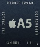
The Apple A5 chip, first introduced on March 11th, 2011, marked a significant evolutionary step in Apple’s silicon development, powering a generation of iconic devices that redefined mobile computing and entertainment. This article provides a comprehensive hardware profile of the A5 series, exploring its architecture, performance characteristics, and the technological context that made it a cornerstone of Apple’s ecosystem during its tenure. While the provided data focuses on a primary iteration of the A5, it’s important to acknowledge that, as with many of Apple’s silicon designs, there were likely variations and refinements throughout its lifespan, catering to different device requirements and manufacturing advancements.
The A5 Chip: A Dual-Core Powerhouse
At its core, the Apple A5 chip is a System on a Chip (SoC) designed by Apple Inc. and manufactured by Samsung. It operates on the ARMv7 instruction set architecture, a 32-bit architecture that was the standard for high-performance mobile processors at the time. The A5 distinguished itself by being one of the first widely adopted dual-core processors in consumer mobile devices, a significant leap from the single-core architectures that preceded it.
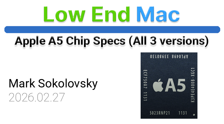
Key Technical Specifications of the Primary A5 Configuration:
- Manufacturer: Samsung
- Release Date: March 11th, 2011
- Codename: APL0498
- Part Number: S5L8940
- Fabrication Process: Initially 45-nanometer, later refined to 32nm High-K dielectric metal gate technology. This transition to a smaller process node is crucial as it typically leads to improved power efficiency and increased transistor density, allowing for more complex designs within a similar physical footprint.
- Transistor Count: While not explicitly stated in the provided data, chips of this era with dual-core ARM Cortex-A9 (or similar) CPUs, integrated GPUs, and memory controllers would typically contain tens of millions to over a hundred million transistors. For context, Apple’s subsequent A6 chip, manufactured on a 32nm process, was estimated to have around 1.04 billion transistors, highlighting the rapid pace of advancement.
- CPU Architecture: ARMv7 (32-Bit)
- CPU Cores:
- Performance Cores: 2
- P-Core Clock Speed: Ranged from 800 MHz to 1 GHz, depending on the specific device and implementation.
- Efficiency Cores: Not present in this configuration, indicating a design focused purely on performance for the primary cores.
- Cache:
- P-Core L1 Instruction Cache: 32 KB per core (64 KB total)
- P-Core L1 Data Cache: 32 KB per core (64 KB total)
- P-Core L2 Cache: 1 MB (shared between the two performance cores). Larger L2 caches are vital for reducing latency by keeping frequently accessed data closer to the CPU cores.
- RAM:
- Memory Type: LPDDR2-800 (running at 400 MHz)
- Memory Bus Width: 64-bit
- Channels: 2 (32-bit per channel)
- Theoretical Bandwidth: Approximately 6.4 GB/s. This bandwidth is critical for feeding data to the CPU and GPU efficiently, especially for demanding tasks like graphics rendering and multitasking.
- Capacity: Typically 512 MB in devices like the iPad 2. This was a substantial amount of RAM for mobile devices at the time, enabling smoother multitasking and more complex applications.
The Graphics Processing Unit (GPU)
The A5 chip integrated a capable graphics processor that was essential for its role in powering visually rich applications, games, and high-definition video playback.
- GPU Cores: 2
- SIMD Units (Execution Units): 4
- FP32 ALUs (Floating Point Arithmetic Logic Units): 32
- GPU Clock Speed: 200 MHz
- Theoretical Performance (FP32 GFLOPS): 12.8 GFLOPS (Giga Floating-point Operations Per Second). This metric provides a benchmark for the raw computational power of the GPU for floating-point operations, crucial for 3D graphics rendering.
Contextualizing the A5: A Timeline of Innovation
The introduction of the A5 chip was not an isolated event but part of Apple’s aggressive roadmap for mobile computing.
- 2007: The first iPhone launches with the Samsung S5L8900 processor, a single-core ARM 11 based chip.
- 2008: The iPhone 3G uses the S5L8900X, an iteration of the original chip.
- 2009: The iPhone 3GS introduces the APL0278, codenamed "Peregrine," a single-core ARM Cortex-A8 processor, representing a significant architectural improvement.
- 2010: The A4 chip (APL0398) powers the iPad and iPhone 4. It’s a single-core ARM Cortex-A8 processor, manufactured on a 45nm process, and a key step in Apple’s in-house silicon strategy.
- March 2011: The Apple A5 chip is unveiled with the iPad 2. This marks the crucial transition to a dual-core architecture, a move that would set the standard for high-end mobile processors for years to come.
- October 2011: The iPhone 4S is released, featuring a variant of the A5 chip, often referred to as the A5R2 or A5S. This iteration likely included optimizations for the smartphone form factor and potentially minor clock speed adjustments.
- March 2012: The third-generation Apple TV utilizes a single-core variant of the A5 chip (codenamed APL2498, part number S5L8947). This demonstrated Apple’s ability to scale its silicon designs for different product needs, optimizing for power and cost.
Devices Powered by the A5 Series
The versatility of the A5 chip allowed it to be integrated into a range of Apple’s popular devices, each leveraging its capabilities in unique ways.
- iPad (2nd generation): This was the flagship device for the initial A5 launch. The dual-core processor, coupled with a more capable GPU and increased RAM, enabled a significantly smoother user experience for browsing, gaming, and productivity applications compared to its predecessor. The iPad 2 was instrumental in solidifying the tablet as a viable computing platform.
- iPhone 4S: While the iPhone 4 had been a marvel with its A4 chip, the iPhone 4S, powered by a variant of the A5, brought a noticeable performance boost. This was critical for handling features like Siri, the new voice assistant that relied heavily on local processing power, and improved camera capabilities.
- Apple TV (3rd generation): As mentioned, a single-core version of the A5 was used here. This was sufficient for the device’s primary functions of streaming media, displaying interfaces, and running simple applications. This demonstrates Apple’s strategic use of its silicon, tailoring it to the specific demands of each product line.
Manufacturing and Design Philosophy
The decision to partner with Samsung for manufacturing was a pragmatic one for Apple during this period. Samsung possessed cutting-edge semiconductor fabrication facilities, allowing Apple to access advanced manufacturing processes like 45nm and subsequently 32nm. This relationship, however, would evolve over time as Apple progressively brought more of its chip design and verification in-house, aiming for greater control over its supply chain and technological roadmap.
The A5’s design, with its dual Cortex-A9-based cores (or Apple’s custom implementation thereof) and a PowerVR SGX543MP2 GPU, represented a balanced approach to performance and power efficiency for its time. The 64-bit memory bus width and dual-channel LPDDR2 memory were key enablers for achieving the impressive memory bandwidth, which is a critical bottleneck in many high-performance computing scenarios.

Impact and Legacy
The Apple A5 chip played a pivotal role in establishing Apple’s dominance in the burgeoning mobile device market.
- Performance Benchmark: The A5 set a new performance standard for smartphones and tablets, demonstrating the tangible benefits of multi-core processing and improved graphics. This pushed competitors to accelerate their own dual-core development efforts.
- Enabling New Features: The processing power of the A5 was directly responsible for the introduction and smooth operation of features like Siri on the iPhone 4S. It also allowed for more sophisticated gaming experiences on iOS devices, transforming them into powerful portable entertainment hubs.
- Ecosystem Growth: The robust performance of devices powered by the A5 fueled the growth of the App Store, encouraging developers to create more demanding and visually rich applications, further cementing the iOS ecosystem’s appeal.
- Foundation for Future Innovation: The A5 served as a crucial stepping stone in Apple’s silicon journey. The lessons learned in designing and optimizing this dual-core architecture directly informed the development of subsequent generations of Apple Silicon, including the A6, A7, and the M-series chips that power Macs today. The transition from ARM Cortex cores to Apple’s own custom CPU designs, which began with the A6, was a strategic move to gain even greater control over performance and efficiency.
Looking Ahead: The Evolution of Apple Silicon
While the A5 represented a significant leap, the pace of technological advancement in the semiconductor industry is relentless. Apple’s commitment to in-house silicon design has been a cornerstone of its strategy, enabling a tightly integrated hardware and software experience. The progression from the A5 to the A-series chips powering iPhones and iPads, and ultimately to the M-series chips that have revolutionized the Mac lineup, showcases Apple’s long-term vision. These later chips feature more cores, advanced architectures (like ARMv8 and beyond), significantly higher transistor counts, dedicated neural engines for AI tasks, and much more sophisticated GPU designs.
The A5, therefore, stands not just as a powerful chip for its era, but as a critical historical marker. It was a product of careful engineering, strategic manufacturing partnerships, and a clear vision for the future of personal computing. Its success validated Apple’s approach to silicon development and laid the groundwork for the unprecedented performance and efficiency that define Apple’s products today. The information detailed in its hardware profile provides a valuable glimpse into the architectural decisions that propelled a generation of devices and shaped the trajectory of the mobile technology landscape.

Source Information:
The provided data originates from a detailed hardware profile of the Apple A5 chip, as documented on a technology-focused website. The specific details regarding the chip’s specifications, including its manufacturing, release date, codename, part number, fabrication process, transistor count (though marked as unavailable), CPU architecture, core counts, clock speeds, cache configurations, RAM specifications, and GPU details, are presented. The source also notes a reference to Apple Silicon on Wikipedia as a primary source for this information, with a retrieval date of February 27th, 2026, indicating a potential archival or updated reference point.
The article acknowledges that there are variations of the A5 chip, citing the Apple TV (3rd generation) as an example of a device utilizing a single-core variant. This detail is important for understanding the scalability and adaptability of Apple’s silicon designs, where a core architecture can be optimized and modified to meet the specific requirements of different product categories. The absence of explicit transistor counts for the A5 itself is a common occurrence for older Apple Silicon specifications, as Apple historically did not readily disclose such figures. However, by comparing it to subsequent generations, we can infer the relative complexity and the rapid advancements made in semiconductor manufacturing.