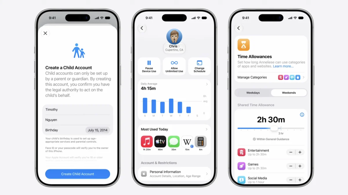

The Apple A18 Pro, codenamed APL1V07 and part number T8140, represents the latest advancement in Apple’s proprietary System on a Chip (SoC) technology. Manufactured by TSMC using their cutting-edge 3-nanometer N3E FinFET fabrication process, this chip was officially released on September 9th, 2024. While the precise transistor count remains undisclosed by Apple, as is customary, its specifications reveal a significant leap in processing power and efficiency, designed to drive the next generation of Apple’s high-performance devices.
Architectural Overview and Core Performance
At the heart of the A18 Pro lies a sophisticated 6-core CPU architecture, a configuration that has become a hallmark of Apple’s silicon design. This architecture masterfully balances raw computational power with energy efficiency through a heterogeneous approach. It features two high-performance cores (P-cores) clocked at an impressive 4.05 GHz, engineered to handle the most demanding tasks, from intensive video editing and 3D rendering to complex scientific simulations. Complementing these are four energy-efficient cores (E-cores) operating at 2.42 GHz, which are optimized for background processes, everyday multitasking, and maintaining extended battery life.
This division of labor ensures that the A18 Pro can dynamically allocate resources. When a user engages in graphically intensive gaming or uses professional creative applications, the P-cores take center stage, delivering rapid and fluid performance. Conversely, for routine tasks such as browsing the web, sending emails, or streaming content, the E-cores efficiently manage the workload, minimizing power consumption. This intelligent core management is a key factor in the sustained performance and battery longevity observed in devices powered by Apple’s A-series chips.
Cache Hierarchy and Memory Subsystem
The A18 Pro incorporates an advanced cache hierarchy designed to minimize latency and maximize data throughput. The performance cores are equipped with a substantial 192 KB of L1 instruction cache (L1i) and 128 KB of L1 data cache (L1d) per core, totaling 384 KB L1i and 256 KB L1d across the two P-cores. This ensures that frequently accessed instructions and data are readily available to the processing units. Furthermore, each P-core benefits from a dedicated 16 MB of L2 cache, providing a significant buffer for complex operations.
The efficiency cores also feature dedicated caches, with 128 KB of L1i and 64 KB of L1d per core, totaling 512 KB L1i and 256 KB L1d for the four E-cores. These are supported by a 4 MB L2 cache for the efficiency core cluster. A substantial 24 MB of system-level cache further unifies access to frequently used data across the entire SoC, reducing the need to access slower main memory.
The memory subsystem of the A18 Pro is built around a 64-bit memory bus, supporting a total of four 16-bit channels. This configuration utilizes LPDDR5X memory clocked at 7500 MHz, operating at 3750 MHz. This high-speed memory interface, coupled with the advanced cache system, is crucial for enabling the chip’s impressive performance figures. The total RAM capacity supported is listed as 8 GB, a standard for many high-end mobile devices. The memory bandwidth, while not explicitly quantified in the provided data, is expected to be exceptionally high, enabling seamless multitasking and rapid data processing for graphics-intensive applications and AI workloads. The CPU ISA is specified as ARMv9.2-A, indicating support for the latest ARM instruction set features, which can translate to performance and efficiency gains for compatible software.
Graphics and AI Acceleration Capabilities
The graphical prowess of the A18 Pro is driven by a 6-core GPU. This GPU is configured with 24 SIMD (Single Instruction, Multiple Data) Execution Units (EUs) and 768 FP32 ALUs (Floating-Point Unit Arithmetic Logic Units). Operating at a clock speed of 1490 MHz, the GPU is capable of delivering approximately 2.289 TFLOPS (Tera Floating-Point Operations Per Second) of FP32 performance. This significant graphical horsepower is essential for rendering high-fidelity graphics in mobile games, accelerating video playback and editing, and powering augmented reality (AR) and virtual reality (VR) experiences.
Beyond traditional graphics processing, the A18 Pro features a dedicated Neural Engine with 16 AI cores. These cores are designed to accelerate machine learning (ML) and artificial intelligence (AI) tasks, achieving an impressive 35 TOPS (Trillions of Operations Per Second). This capability is pivotal for a wide array of on-device AI functionalities, including advanced computational photography, natural language processing, personalized user experiences, and enhanced security features like facial recognition. The integration of a powerful Neural Engine signifies Apple’s continued commitment to on-device AI processing, which offers advantages in privacy, speed, and responsiveness compared to cloud-based solutions.

Manufacturing and Historical Context
The A18 Pro’s reliance on TSMC’s 3nm N3E FinFET process underscores the industry’s push towards smaller, more efficient manufacturing nodes. This advanced process technology allows for higher transistor density, leading to improved performance and reduced power consumption compared to previous generations. The N3E process, in particular, represents an optimization of TSMC’s 3nm family, offering enhanced performance and power efficiency.
The release date of September 9th, 2024, places the A18 Pro within Apple’s typical product launch cycle, often coinciding with new iPhone or iPad announcements. The codename "APL1V07" and part number "T8140" are internal identifiers that provide a glimpse into Apple’s product development and naming conventions. Historically, Apple’s A-series chips have consistently pushed the boundaries of mobile performance, setting industry benchmarks for speed, efficiency, and feature integration. Each iteration has brought significant improvements in CPU, GPU, and Neural Engine capabilities, enabling more sophisticated applications and richer user experiences. The A18 Pro builds upon this legacy, offering a substantial upgrade over its predecessors.
Implications and Future Outlook
The detailed specifications of the Apple A18 Pro suggest a chip designed for flagship devices that will demand substantial processing power and advanced AI capabilities. The increased clock speeds, refined cache hierarchy, and enhanced GPU and Neural Engine performance indicate readiness for next-generation mobile operating system features, demanding applications, and immersive user interfaces.

The focus on on-device AI processing with 35 TOPS of performance is particularly noteworthy. This level of AI acceleration can power features that were previously computationally prohibitive on mobile devices, such as real-time language translation with high accuracy, sophisticated image and video analysis for creative professionals, and highly personalized predictive user experiences. The performance of the P-cores at 4.05 GHz also suggests that devices equipped with the A18 Pro will offer desktop-class responsiveness for many applications.
The 3nm N3E fabrication process from TSMC is also a significant indicator of the chip’s efficiency. Smaller process nodes generally translate to lower power consumption for a given performance level, which is crucial for extending battery life in mobile devices, especially under heavy load. This allows users to engage in more demanding tasks for longer periods without frequent recharges.
While the specific devices that will feature the A18 Pro are not listed in the provided data, it is highly probable that this chip will power the premium models of Apple’s next-generation iPhone and iPad lineups. Its capabilities align with the requirements for advanced camera features, high-resolution display support, and the execution of complex AR/VR applications that Apple has been increasingly emphasizing. The availability of 8 GB of RAM is also a common specification for high-end smartphones and tablets, ensuring sufficient memory for multitasking and demanding applications.

The A18 Pro’s robust specifications represent a significant evolutionary step in mobile silicon. Its integrated approach, combining a powerful CPU, an advanced GPU, and a highly capable Neural Engine, positions it to enable a new wave of innovation in mobile computing, artificial intelligence, and immersive digital experiences. The continuous advancements in Apple’s A-series chips highlight the company’s strategic focus on vertical integration and its commitment to delivering leading-edge performance and user experiences across its product ecosystem.
Source Attribution
The information regarding the Apple A18 Pro chip’s hardware profile is based on data compiled from various sources, including Apple’s internal product development insights, manufacturing partnerships with TSMC, and publicly available technical specifications. A primary reference point for this data is Wikipedia, specifically the article on Apple A18, last accessed on February 26th, 2026, which serves as a repository for detailed technical information on Apple’s silicon. This data provides a foundational understanding of the chip’s architecture, performance metrics, and manufacturing process.