
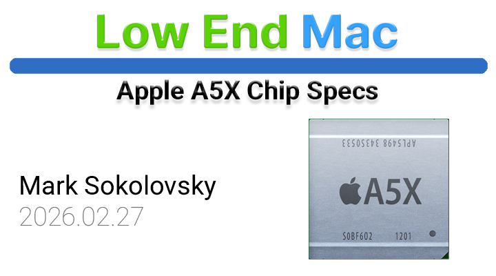
The Apple A5X System-on-Chip (SoC) represents a significant milestone in mobile processing technology, marking a pivotal point in Apple’s strategy to deliver enhanced performance and graphics capabilities to its flagship devices. Released on March 16th, 2012, and manufactured by Samsung using a 45-nanometer fabrication process, the A5X chip was a direct evolution of its predecessor, the A5, with a particular emphasis on graphical prowess. This detailed hardware profile examines the architectural components of the A5X, its technical specifications, and its role in shaping the user experience of the devices it powered, primarily the third-generation iPad.
Architectural Foundation and Core Components
At its heart, the Apple A5X SoC is built upon the ARMv7 architecture, supporting 32-bit processing. This instruction set architecture (ISA) was the industry standard for high-performance mobile devices at the time, providing a robust and efficient foundation for complex computations. The chip features a dual-core CPU configuration, with each of the two performance cores operating at a clock speed of 1 GHz. This configuration offered a substantial boost in processing power compared to previous generations, enabling smoother multitasking and faster application performance.
While the A5X featured two high-performance cores, it did not incorporate efficiency cores, a design choice that prioritized raw power for demanding tasks over aggressive power saving. This approach was well-suited for a tablet device like the iPad, where sustained performance for graphics-intensive applications and media consumption was a primary user expectation.
Memory Subsystem: Enabling Enhanced Graphics Performance
A key differentiator of the A5X chip, particularly when compared to its contemporary mobile processors, was its advanced memory subsystem. The chip boasted a 128-bit memory bus width, a considerable increase that allowed for significantly higher data throughput. This was achieved through four independent 32-bit channels, enabling parallel access to memory and reducing latency. The memory type employed was LPDDR2-800, operating at a frequency of 400 MHz. This combination of a wide bus and fast memory delivered an impressive theoretical bandwidth of approximately 12.8 GB/s.
This substantial memory bandwidth was crucial for the A5X’s primary objective: to power the Retina display of the third-generation iPad. The high pixel density of the Retina display required a graphics processor capable of rendering a massive number of pixels quickly and efficiently. The A5X’s memory architecture was specifically designed to feed the GPU with the data it needed to achieve this, ensuring a fluid and responsive visual experience even with high-resolution graphics and complex visual elements. The chip was equipped with 512 MB of RAM, a capacity that, while modest by today’s standards, was considered generous for its time and sufficient to support the demanding graphical tasks the A5X was engineered for.
Graphics Processing Unit: A Leap in Visual Capabilities
The graphics capabilities of the A5X were a significant upgrade, designed to handle the visual fidelity demanded by the iPad’s Retina display. The SoC integrated a powerful GPU featuring four cores. While specific details on the exact architecture of this GPU are not as widely publicized as CPU cores, it was understood to be a custom design from Apple, likely based on a PowerVR architecture. It featured 8 SIMD (Single Instruction, Multiple Data) execution units and 64 FP32 (Floating-Point Single Precision) ALUs (Arithmetic Logic Units).
Operating at a clock speed of 200 MHz, the GPU was capable of delivering approximately 25.6 GFLOPS (Giga Floating-point Operations Per Second). This computational power was a substantial leap forward, enabling more complex visual effects, smoother animations, and faster rendering of high-resolution graphics. The dual-core CPU, coupled with this robust GPU and the high-bandwidth memory, allowed the third-generation iPad to excel in gaming, video playback, and graphically intensive applications, setting a new benchmark for tablet performance at its release.

Manufacturing and Timeline
The Apple A5X SoC was manufactured by Samsung, a long-standing partner of Apple in semiconductor production. The use of a 45-nanometer fabrication process was at the cutting edge of semiconductor manufacturing at the time of its release, allowing for a balance of performance and power efficiency. The chip carries the codename APL5498 and the part number S5L8945, internal identifiers used by Apple and its manufacturing partners.
The release date of March 16th, 2012, aligns with the launch of the third-generation iPad, which was the primary device to feature this new SoC. This strategic timing allowed Apple to equip its latest tablet with a chip that could effectively drive its new Retina display, a key marketing and user-experience differentiator.
The Context of the A5X: Pushing the Boundaries of Mobile Computing
The release of the A5X chip was not an isolated event but part of Apple’s broader strategy to continually advance the capabilities of its mobile devices. In 2012, the tablet market was still in its relatively early stages, with devices like the iPad defining the category. The introduction of the Retina display on the third-generation iPad was a bold move, requiring a significant increase in processing power, particularly in graphics. The A5X was engineered precisely to meet this demand.
Prior to the A5X, the A5 chip, found in the iPhone 4S and the second-generation iPad, had already demonstrated Apple’s prowess in designing powerful mobile processors. However, the A5X represented a specialized evolution, doubling down on graphical performance to support the unprecedented pixel density of the Retina display. This focus on integrated graphics was a key trend in mobile SoC design, as devices were increasingly used for entertainment, gaming, and media consumption, all of which are heavily reliant on GPU performance.

The decision to manufacture the chip using Samsung’s 45nm process was typical of the industry at the time. While smaller nanometer processes offer greater efficiency and performance, 45nm provided a mature and reliable platform for high-volume production, balancing cost and technological advancement.
Implications and Broader Impact
The Apple A5X SoC had a profound impact on the mobile computing landscape, primarily by enabling the successful integration of the Retina display into the third-generation iPad. This paved the way for higher resolution displays across a wider range of devices, setting a new standard for visual clarity. The enhanced graphical capabilities also contributed to a richer and more immersive gaming and application experience on the iPad, solidifying its position as a powerful entertainment and productivity device.
The architecture of the A5X, with its focus on memory bandwidth to support graphics, highlighted a crucial aspect of mobile SoC design: the interconnectedness of CPU, GPU, and memory. This demonstrated that raw CPU clock speed alone was not sufficient for cutting-edge mobile performance; a balanced system architecture was essential.
Furthermore, the A5X, as part of Apple’s in-house silicon development, underscored the company’s commitment to vertical integration. By designing its own chips, Apple could tailor hardware and software to work in perfect synergy, optimizing performance, power efficiency, and user experience. This strategy has been a cornerstone of Apple’s success and continues to define its product development.

While the A5X was a powerful chip for its time, it was eventually succeeded by more advanced processors, such as the A6X and subsequent generations of Apple Silicon. However, its contribution to the evolution of mobile graphics and display technology remains undeniable. It served as a testament to Apple’s engineering capabilities and its relentless pursuit of delivering premium user experiences through cutting-edge hardware. The architectural choices made in the A5X, particularly its emphasis on memory bandwidth for graphics, laid important groundwork for future advancements in mobile SoC design, influencing the development of more powerful and visually capable smartphones and tablets for years to come.
Further Technical Details and Comparisons
To further contextualize the A5X, it’s useful to consider its place within the evolution of Apple’s A-series chips. The A5X was a direct successor to the A5, which featured a dual-core ARM Cortex-A9 CPU and a PowerVR SGX543MP2 GPU. The A5X retained the dual-core ARMv7 CPU architecture but significantly upgraded the GPU to what is widely believed to be a PowerVR SGX543MP4, effectively doubling the GPU cores from two to four. This core doubling, combined with the increased memory bandwidth, was the primary driver behind its enhanced graphics performance.
The 45-nanometer fabrication process, while advanced for 2012, was a step in the ongoing miniaturization of transistors. Newer processes, such as 32nm and eventually 28nm and below, would offer further improvements in power efficiency and performance density in subsequent chip generations. The transistor count for the A5X is not publicly disclosed, a common practice for Apple’s custom silicon, but it would have been considerably higher than the A5 due to the more complex GPU.
The absence of efficiency cores on the A5X, while providing peak performance, also meant that it might have consumed more power during less demanding tasks compared to chips with heterogeneous cores (a design that became more prevalent in later mobile processors, including Apple’s own). This trade-off was likely deemed acceptable for the target device, the iPad, which often had access to a larger battery and was used for sustained, graphically intensive activities.

Conclusion
The Apple A5X System-on-Chip stands as a crucial piece of Apple’s silicon history, a testament to its ability to innovate and push the boundaries of mobile technology. Released in 2012, it was a carefully engineered solution to meet the demands of the then-revolutionary Retina display, providing a significant leap in graphical performance through its enhanced GPU and high-bandwidth memory architecture. While specific details like transistor count remain proprietary, the publicly available specifications paint a clear picture of a chip designed for power and visual fidelity. Its impact extended beyond the devices it powered, influencing the trajectory of mobile display technology and reinforcing Apple’s strategic advantage through custom silicon development. The A5X was not just a component; it was an enabler of a premium user experience that helped define the modern tablet.