
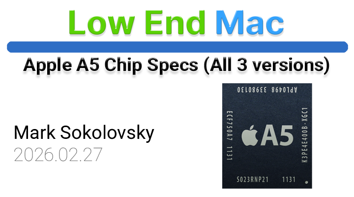
The Apple A5 chip, a significant advancement in mobile processing, represents a pivotal moment in Apple’s silicon development trajectory. This dual-core processor, manufactured by Samsung, was first introduced on March 11th, 2011, marking a substantial leap in performance and efficiency for the devices it powered. This detailed examination delves into the intricate hardware specifications of the A5 series, exploring its architecture, capabilities, and the broader context of its release and subsequent impact on the mobile computing landscape.
Unpacking the A5 Architecture: Core Components and Specifications
At the heart of the Apple A5 chip lies its dual-core CPU, based on the ARMv7 instruction set, capable of 32-bit processing. This configuration provided a considerable performance boost over its single-core predecessors, enabling smoother multitasking and more demanding application execution. The A5 chip typically operated at clock speeds ranging from 800 MHz to 1 GHz, a significant increase that directly translated to enhanced responsiveness in user interfaces and faster processing for applications.
The CPU’s cache hierarchy was a critical element in its performance. Each of the two performance cores was equipped with 32 KB of L1 instruction cache (L1i) and 32 KB of L1 data cache (L1d), totaling 64 KB of L1 cache per core. This per-core cache design minimized latency by keeping frequently accessed data and instructions close to the processing units. Furthermore, the A5 featured a 1 MB L2 cache shared between the performance cores, providing an additional layer of fast memory for data and instructions that couldn’t be accommodated in the L1 caches. This multi-level cache system was instrumental in maintaining high performance even under heavy computational loads.
The A5 chip also incorporated a dual-core GPU (Graphics Processing Unit) designed to handle the graphical demands of modern mobile applications and high-definition media playback. This GPU featured 4 SIMD (Single Instruction, Multiple Data) execution units and 32 FP32 (Floating-Point Single Precision) arithmetic logic units (ALUs), operating at a clock speed of 200 MHz. This configuration delivered approximately 12.8 Gigaflops (GFLOPS) of theoretical floating-point performance, a crucial metric for rendering complex graphics, accelerating video decoding, and enabling more immersive gaming experiences on mobile devices.
Memory and Fabrication: The Foundation of Performance
The A5 chip was paired with LPDDR2-800 memory, operating at 400 MHz. This memory subsystem utilized a 64-bit wide memory bus, divided into two 32-bit channels. This architecture provided a theoretical memory bandwidth of 6.4 GB/s, a substantial figure for its time, ensuring that the CPU and GPU had rapid access to the data they needed. The standard configuration for devices featuring the A5 chip included 512 MB of RAM, which was ample for the operating systems and applications of the era, facilitating smooth transitions between tasks and robust multitasking capabilities.

The fabrication process of the A5 chip showcased Apple’s commitment to cutting-edge manufacturing. Initially produced using a 45-nanometer process, later iterations adopted the more advanced 32nm High-K dielectric metal gate process. This transition to a smaller fabrication node offered significant advantages, including reduced power consumption, improved transistor density, and higher clock speeds, all contributing to a more power-efficient and performant chip. While the exact transistor count for the A5 chip has not been publicly disclosed by Apple, such advancements in fabrication typically lead to a substantial increase in transistor density, enabling more complex functionality within a smaller physical footprint.
A Tale of Three Variations: The A5 Family
It’s important to note that the Apple A5 designation encompasses at least three distinct variations, each tailored for specific device requirements. While the core architecture remained similar, subtle differences in clock speeds, core configurations, or power management could exist between these variants. For instance, the A5 chip utilized in the third-generation Apple TV was notably different, featuring a single CPU core instead of the typical two, and a reduced L1 cache (32 KB L1i and 32 KB L1d per core) compared to its iPhone and iPad counterparts. This optimization was likely driven by the specific power and performance demands of the Apple TV’s use case, prioritizing efficiency and cost-effectiveness for a set-top box.
Historical Context and Market Impact
The introduction of the Apple A5 chip in 2011 coincided with a rapidly evolving mobile technology landscape. The iPhone 4S, released in October 2011, was one of the first devices to feature this powerful new processor. The A5 chip was instrumental in enabling features like 1080p video recording and playback, a significantly improved camera experience, and the introduction of Siri, Apple’s intelligent personal assistant, which relied heavily on the chip’s processing power.

The iPad 2, launched earlier in March 2011, also prominently featured the A5 chip. This enabled a much thinner and lighter design compared to its predecessor, along with substantial performance gains that made the tablet a more compelling device for productivity and entertainment. The A5 chip allowed the iPad 2 to handle more complex web browsing, richer gaming experiences, and smoother video playback, solidifying its position as a leader in the burgeoning tablet market.
The A5’s dual-core architecture and improved graphics capabilities were key differentiators, allowing Apple to offer devices that were not only faster but also more capable of running the increasingly sophisticated apps being developed for iOS. This era marked a crucial period where mobile devices began to rival, and in some cases surpass, the performance of traditional desktop computers for many common tasks.
Manufacturing and Supply Chain Dynamics
The manufacturing of the Apple A5 chip by Samsung highlights the complex and interconnected nature of the global semiconductor supply chain. At the time, Samsung was a leading foundry for advanced chip manufacturing, and their partnership with Apple for the A-series chips was a critical component of Apple’s product strategy. This relationship, while fruitful for both companies, also underscored the strategic importance of secure and reliable manufacturing partnerships for tech giants. The reliance on a single foundry for such critical components also presented potential vulnerabilities, as evidenced by later industry discussions and shifts in Apple’s supply chain strategy.

Analysis of Implications: A Foundation for Future Innovation
The Apple A5 chip was more than just an incremental upgrade; it was a foundational piece of technology that enabled a new generation of mobile devices. Its dual-core design set a precedent for the multi-core architectures that would become standard in the industry. The enhanced graphics capabilities paved the way for more visually rich and interactive mobile experiences.
The success of the A5 chip also solidified Apple’s strategy of designing its own silicon in-house, a move that allowed for tighter integration between hardware and software, leading to optimized performance and unique user experiences. This vertical integration strategy has since become a hallmark of Apple’s product development, enabling them to push the boundaries of what is possible in mobile computing.
The A5’s efficiency, stemming from its advanced fabrication process and architecture, was also crucial for battery life, a perennial concern for mobile devices. By delivering more performance per watt, Apple could create devices that offered both power and longevity, further enhancing their appeal to consumers.

Looking Back: The Legacy of the A5
While newer generations of Apple Silicon have surpassed the A5 in raw performance, its historical significance cannot be overstated. The A5 chip was a critical stepping stone, demonstrating Apple’s prowess in chip design and manufacturing. It powered some of the most iconic Apple devices of its era and played a crucial role in shaping the mobile computing landscape as we know it today. The technical specifications detailed herein—the dual-core ARMv7 CPU, the capable GPU, the efficient memory subsystem, and the advanced fabrication process—collectively represent a powerful and influential piece of mobile technology that left an indelible mark on the industry. The A5 chip’s legacy is one of innovation, performance, and the relentless pursuit of technological excellence that continues to define Apple’s approach to silicon development.