Before Apple revolutionized personal computing with its custom silicon, the earliest iOS devices relied on chips manufactured by Samsung. This foundational period paved the way for Apple’s ambitious in-house chip development, a journey that began with the A4 chip and has since evolved into the formidable A-Series System on a Chip (SoC) architecture that powers every iPad and iPhone since 2010. This article chronicles the remarkable progression of Apple’s A-Series chips, from their humble beginnings to the cutting-edge processors of today, and projects into the future with the anticipated advancements.
The Genesis: Samsung’s Role and the Dawn of Apple Silicon
In the nascent stages of the iPhone and iPad, Samsung was the chosen partner for providing the crucial processing units. These early chips, while instrumental in the initial success of Apple’s mobile devices, were a far cry from the integrated marvels we see today. The transition to in-house design marked a pivotal moment, granting Apple unprecedented control over its hardware and software integration, a strategic advantage that has defined its product ecosystem.
The designation "A-Series" emerged around 2010, signifying Apple’s commitment to a standardized naming convention for its custom-designed SoCs. This move not only streamlined internal development but also provided a clear evolutionary path for consumers and industry observers alike. The underlying philosophy has remained consistent: to push the boundaries of mobile processing power, efficiency, and graphics capabilities, thereby enhancing the user experience and enabling new functionalities.
The First Steps: A1, A2, and A3 – Laying the Foundation
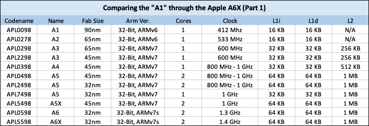
The earliest iterations of Apple’s custom silicon were marked by their integration of Samsung’s foundational architecture. The chip often referred to as the "Apple A1," technically identified as "APL0098" or the Samsung S5L8900, powered the very first iPhone, iPod touch, and iPhone 3G. This 32-bit ARMv6 processor, fabricated on a 90-nanometer process, operated at a modest 412 MHz, a significant underclock from its potential 666 MHz. Its cache configuration was basic, featuring 16 KB of L1 Instruction and 16 KB of L1 Data cache, with no L2 or L3 cache. Memory bandwidth was limited to 533 MB/s, facilitated by 128 MB of 133.25 MHz LPDDR-266 RAM. The design prioritized power efficiency, a critical factor for early mobile devices grappling with battery life limitations.
While there wasn’t an official "Apple A2" chip, this designation is often attributed to the processor found in the second-generation iPod touch. This chip was a refinement of the A1, moving to a more advanced 65-nanometer fabrication process, hinting at future improvements in efficiency and performance.
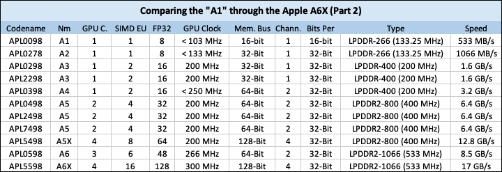
The "Apple A3," identified by the S5L8920 and S5L8922 designations, represented a significant leap forward. Found in the iPhone 3GS and the third-generation iPod touch, this chip doubled the L1 cache to 32 KB per core. Crucially, it introduced a 256 KB L2 cache, a feature notably absent in its predecessors, which dramatically improved instruction processing and overall responsiveness. Memory bandwidth doubled to 1.6 GB/s, supported by 256 MB of LPDDR-400 (200 MHz) RAM. The GPU clock speed was also boosted to 200 MHz, marking an important step in enhancing graphical capabilities.
The A4: Apple’s In-House Design Takes Center Stage
The introduction of the A4 chip in 2010, powering the iPhone 4, iPad, and fourth-generation iPod touch, marked Apple’s definitive move towards in-house silicon design, mirroring the ethos of its later "Apple Silicon" initiatives. While still a 32-bit processor, the A4 significantly enhanced performance over the previous generation. It featured a 512 KB L2 cache, a substantial increase from the A3, and CPU clock speeds ranging from 800 MHz to 1 GHz, depending on the device. Memory bandwidth saw a considerable uplift to 3.2 GB/s. This chip established Apple’s independent trajectory in processor development, laying the groundwork for future innovations.

The A5 and A5X: Dual-Core Power and Enhanced Graphics
The A5 chip, introduced with the second-generation iPad in March 2011, brought dual-core processing to Apple’s mobile devices. Apple touted its ability to "do twice the work" of the A4, with a ninefold increase in graphical performance. All A5 and A5X chips featured a 1 MB L2 cache, a substantial upgrade. The A5X, powering the third-generation iPad, was a high-performance variant designed for demanding graphical tasks, boasting a quad-core graphics chip that delivered approximately 25.6 Gigaflops of graphical processing power, a significant jump for mobile devices at the time. This generation showcased Apple’s increasing focus on parallel processing and graphics acceleration.
The A6 and A6X: Breaking the 1 GHz Barrier and LPDDR2 Adoption
With the A6 and A6X chips, Apple further pushed performance boundaries. The A6, found in the iPhone 5 and 5c, achieved CPU clock speeds of 1.3 GHz. The A6X, powering the fourth-generation iPad, reached 1.4 GHz. This generation also saw an upgrade in RAM technology to LPDDR2-1066, resulting in memory bandwidth of 8.5 GB/s for iPhones and an impressive 17 GB/s for the fourth-generation iPad. GPU clock speeds also saw incremental improvements, reaching 266 MHz on iPhones and 300 MHz on the iPad 4.
The A7: The 64-Bit Revolution in Mobile
September 10, 2013, marked a watershed moment with the introduction of the A7 chip. This was the world’s first 64-bit mobile SoC, a groundbreaking architectural shift that enabled more complex computations and increased memory addressing capabilities. The A7 powered devices like the iPhone 5s, iPad mini 2, iPad mini 3, and the original iPad Air. Fabricated on an even smaller process node, it contained over one billion transistors, delivering substantial performance improvements over its 32-bit predecessors. This transition to 64-bit architecture set a new standard for mobile computing and future-proofed Apple’s devices for years to come.
The A8: Enabling Larger iPhones and Enhanced Popularity
The A8 chip arrived with the highly popular iPhone 6 and 6 Plus. These devices, which became Apple’s most successful iPhone models to date, selling approximately a quarter of a billion units globally, relied on the A8 for their performance. While specific technical details of the A8’s internal architecture are less publicly detailed than some other generations, it represented a continued evolution in processing power and efficiency, catering to the demands of larger displays and enhanced user experiences. The widespread adoption of the iPhone 6 and 6 Plus underscored the importance of a robust and reliable processor in driving mass-market success.
The A9, A9X, and the Shift to TSMC
The A9 chip introduced a significant change in manufacturing. While an initial version was produced by Samsung, a subsequent iteration was manufactured by TSMC (Taiwan Semiconductor Manufacturing Company). This partnership marked a strategic diversification for Apple’s supply chain. The A9 powered the iPhone 6s, 6s Plus, and the iPhone SE. It was also the first Apple device to utilize DDR4 RAM, predating its adoption in Macs by several years.
A key innovation with the A9 was the introduction of an Apple-designed NVMe controller, incorporating PCI Express technology. This custom storage solution dramatically increased internal storage speeds, a critical upgrade for handling larger apps, higher-resolution photos, and 4K video. This marked a new era of faster internal storage on iPhones. The A9X, a more powerful variant, continued this trend of enhanced performance for tablets.
The A10 Fusion and A10X Fusion: Efficiency Cores and Quad-Core Power
September 16, 2016, saw the release of the iPhone 7 and 7 Plus, powered by the A10 Fusion chip. This marked another significant architectural advancement: the introduction of "Efficiency Cores." The A10 Fusion was Apple’s first quad-core SoC, featuring two high-performance cores and two high-efficiency cores. This innovative design allowed the chip to intelligently switch between cores based on the task at hand, optimizing power consumption without compromising performance. Apple claimed a 40% improvement in CPU performance and a 50% increase in GPU performance over the A9. The A10X Fusion, powering the 2016 iPad Pro, offered even greater processing and graphics capabilities.
The T2 Chip: A Specialized Security and Control Co-Processor
While not part of the A-Series line directly, the T2 chip’s emergence is noteworthy in the context of Apple’s integrated silicon strategy. Introduced in Mac computers, the T2 chip acts as a co-processor, handling critical functions such as secure boot, encrypted storage, and image signal processing. Its presence signifies Apple’s growing commitment to dedicated, specialized silicon for enhanced security and system control, a philosophy that has increasingly permeated its entire product lineup.
The Path Forward: A19 and Beyond – Desktop-Class Performance
Looking towards the future, by 2026, the iPhone 17 lineup is anticipated to feature the A19 and A19 Pro chips. These processors are expected to deliver "desktop-class" multicore processing, graphics power, and responsiveness. While current mobile Apple SoCs already compete effectively with chips like the M1, the trajectory of the A-Series indicates a consistent, incremental build-up of performance and efficiency. The future promises even more integrated, powerful, and efficient chips that will continue to redefine the capabilities of smartphones and tablets, blurring the lines between mobile and desktop computing.
The evolution of Apple’s A-Series chips is a testament to the company’s relentless pursuit of technological innovation. From its early reliance on external manufacturers to its current position as a leader in custom silicon design, Apple has consistently leveraged its in-house chip development to create powerful, efficient, and integrated devices that shape the landscape of personal technology. Each iteration has not only enhanced performance but also enabled new features and user experiences, solidifying Apple’s position as a dominant force in the global tech industry.