
The Apple A5 chip, a pivotal component in the evolution of Apple’s mobile device ecosystem, represents a significant leap in processing power and efficiency for its time. This article provides a comprehensive hardware profile of the A5 series, detailing its architecture, performance metrics, and the technological context of its release. While the provided data focuses on a specific iteration, the A5 family encompassed variations that powered some of Apple’s most influential products, including the iPad 2, iPhone 4S, and the third-generation Apple TV. Understanding the A5 is crucial for appreciating the foundational advancements that paved the way for the sophisticated silicon powering today’s ubiquitous Apple devices.
Genesis and Architecture of the A5 Chip
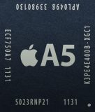
The Apple A5 chip, primarily manufactured by Samsung, made its debut on March 11th, 2011, marking a significant upgrade from its predecessor, the A4. Codenamed APL0498 and bearing the part number S5L8940, the A5 was engineered with a dual-core design, a departure from the single-core architecture of the A4. This fundamental shift in design philosophy was aimed at delivering a substantial boost in both computational throughput and graphical capabilities, essential for the increasingly demanding applications and user experiences emerging on iOS.
The fabrication process for the A5 chip was noteworthy for its time, utilizing either a 45-nanometer or a more advanced 32nm High-K dielectric metal gate process. This shrink in manufacturing technology allowed for greater transistor density, leading to improved power efficiency and performance within a smaller physical footprint. While the exact transistor count for the A5 is not explicitly detailed in the provided data, such advancements in fabrication typically correlate with a significant increase in the number of transistors, enabling more complex circuitry and enhanced functionality.
At its core, the A5 chip employed the ARMv7 instruction set architecture (ISA), a 32-bit architecture widely adopted for mobile and embedded systems due to its balance of performance and power efficiency. The dual-core configuration of the A5 was a key differentiator. It featured two performance cores (P-cores) that could operate at clock speeds ranging from 800 MHz to 1 GHz. This dual-core approach allowed for parallel processing, enabling devices to handle multiple tasks simultaneously with greater fluidity, a crucial enhancement for multitasking and more demanding applications.
Memory Subsystem and Bandwidth
The memory subsystem of the A5 chip was designed to support its dual-core processing capabilities. It utilized a 64-bit memory bus, providing a robust pipeline for data transfer between the CPU and RAM. This bus was configured with two channels, each 32 bits wide, contributing to the overall bandwidth. The A5 incorporated LPDDR2-800 memory, operating at 400 MHz. This type of RAM is known for its lower power consumption and higher speeds compared to earlier generations, making it an ideal choice for battery-powered mobile devices.
The memory bandwidth for the A5 was estimated at approximately 6.4 GB/s. This figure represents the theoretical maximum rate at which data could be transferred between the processor and the memory. For a device in 2011, this level of bandwidth was substantial and played a critical role in ensuring that the dual-core CPU could be fed with data efficiently, preventing bottlenecks and maximizing the performance gains offered by the dual-core architecture. The typical RAM capacity found in devices equipped with the A5 was 512 MB, a standard for high-end mobile devices at the time.
CPU Core Details and Cache Hierarchy
The CPU configuration of the A5 chip was characterized by its two performance cores. Each of these cores was equipped with dedicated L1 caches: a 32 KB L1 instruction cache (L1i) and a 32 KB L1 data cache (L1d). This per-core cache design allows for rapid access to frequently used instructions and data, minimizing the need to fetch information from slower main memory. Consequently, the total L1 cache for the dual-core configuration was 64 KB for both instructions and data.
A notable exception existed for the Apple TV (3rd generation), which featured a single-core variant of the A5. In this specific implementation, the L1 caches were halved, with each core (or the single core in this case) having 32 KB of L1i and 32 KB of L1d cache.
Beyond the L1 caches, the A5 also featured a shared L2 cache. The provided data indicates a 1 MB L2 cache for the performance cores, shared between them. This larger cache serves as a secondary buffer for frequently accessed data, further reducing latency and improving overall CPU performance. The absence of efficiency cores (E-cores) in the A5 design means that all processing was handled by these performance cores, prioritizing raw speed and responsiveness for the tasks at hand. The clock speeds of these performance cores could dynamically adjust, typically ranging from 800 MHz to 1 GHz, allowing for a balance between power consumption and performance needs.
Integrated Graphics Performance
The graphical capabilities of the A5 chip were handled by an integrated PowerVR SGX543MP2 GPU. This GPU featured two cores, which were further subdivided into execution units (EUs) and floating-point arithmetic logic units (ALUs). The data indicates 4 SIMD (Single Instruction, Multiple Data) EUs and 32 FP32 ALUs. The GPU operated at a clock speed of 200 MHz.
The theoretical peak performance of the GPU was measured in floating-point operations per second (FLOPS). For the A5, this was calculated at 12.8 GFLOPs (GigaFLOPS). This level of graphical processing power was significant for 2011, enabling smooth rendering of complex 2D and 3D graphics, high-definition video playback, and the execution of graphically intensive applications and games that were becoming increasingly prevalent on iOS devices. The inclusion of a capable GPU was essential for delivering the rich visual experiences that Apple users had come to expect.

Timeline and Product Integration
The Apple A5 chip’s introduction in March 2011 coincided with the launch of the second-generation iPad. This marked a significant upgrade for the iPad, bringing a substantial increase in processing speed and graphical performance, which translated into a smoother and more responsive user experience for browsing, gaming, and productivity tasks.
Later that year, in October 2011, the A5 chip powered the iPhone 4S. This iteration of the iPhone was a landmark device, introducing Siri, Apple’s intelligent voice assistant, which heavily relied on the enhanced processing power of the A5 for its natural language processing capabilities. The dual-core A5 ensured that Siri could function effectively while the device concurrently handled other operations.
The third-generation Apple TV, released in March 2012, also featured a derivative of the A5 chip. As previously noted, this version of the A5 was a single-core variant, likely optimized for the specific power and performance requirements of a set-top streaming device. This allowed for efficient operation of the Apple TV’s interface and its streaming capabilities without the need for the full dual-core power of its siblings.
Context and Implications
The release of the Apple A5 chip occurred during a period of intense competition and rapid innovation in the mobile computing landscape. The smartphone and tablet markets were burgeoning, with companies vying to offer devices with increasingly powerful processors to support richer software experiences. Apple’s strategy of designing its own custom silicon, rather than relying solely on off-the-shelf components, allowed it to tightly integrate hardware and software, optimizing performance and efficiency in a way that was difficult for competitors to replicate.

The dual-core architecture of the A5 was a strategic move to keep pace with the evolving demands of mobile applications. As developers began to explore more complex functionalities, from advanced gaming to sophisticated productivity tools, the need for greater computational power became paramount. The A5 provided this power, enabling a smoother and more capable user experience across Apple’s flagship devices.
The efficiency gains, partly due to the 32nm process and LPDDR2 memory, were also critical. In battery-powered devices, maximizing performance while minimizing power consumption is a constant challenge. The A5 represented a significant step forward in this regard, contributing to longer battery life and sustained performance during demanding usage.
The A5 chip’s success laid the groundwork for future Apple Silicon development. The lessons learned in designing and manufacturing the A5, particularly regarding dual-core architecture, memory management, and integrated graphics, were instrumental in the subsequent generations of A-series chips. These advancements not only propelled Apple’s own product lines forward but also influenced the broader trajectory of mobile processor design, pushing the industry towards more powerful, efficient, and integrated System-on-a-Chip (SoC) solutions.
Broader Impact and Legacy
The Apple A5 chip was more than just a collection of transistors; it was a crucial enabler of key Apple products that shaped the mobile computing landscape. The iPad 2, with its significantly improved performance thanks to the A5, solidified the tablet as a viable computing platform for a wide range of users. The iPhone 4S, powered by the A5, brought advanced features like Siri to the masses, demonstrating the potential of intelligent software integrated with powerful hardware.

The A5 chip’s legacy is intrinsically linked to the rise of the iOS ecosystem. Its performance allowed for the development and widespread adoption of applications that demanded more processing power, from high-fidelity games to sophisticated creative tools. This, in turn, fueled the App Store’s growth and solidified Apple’s position as a leader in the mobile market.
While newer generations of Apple Silicon have since surpassed the A5 in raw performance, its contribution remains significant. It represented a pivotal moment where Apple transitioned from single-core to dual-core processing in its mainstream mobile devices, a fundamental architectural shift that defined the performance characteristics of its products for years to come. The A5 chip stands as a testament to Apple’s early prowess in custom silicon design and its commitment to pushing the boundaries of mobile technology, setting a high bar for performance, efficiency, and integration.
Source: (Apple Silicon, Wikipedia, the free encyclopedia, https://en.wikipedia.org/wiki/Apple_silicon, February 27th, 2026.)