 Vera Clarissa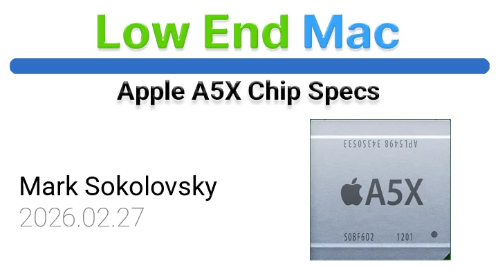
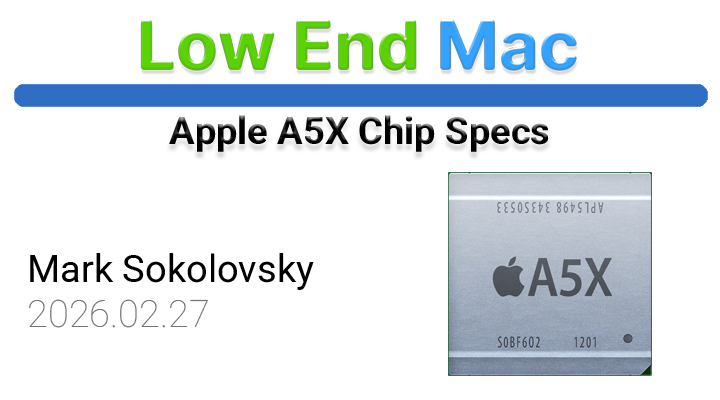
The Apple A5X System-on-a-Chip (SoC) represents a significant evolutionary step in Apple’s mobile processor design, specifically engineered to enhance graphical capabilities and overall performance for its flagship devices of the early 2010s. Launched on March 16th, 2012, and manufactured by Samsung using a 45-nanometer fabrication process, the A5X was a pivotal component that powered the third-generation iPad, distinguishing it with a substantial boost in visual fidelity and processing power compared to its predecessors. This detailed examination delves into the intricate hardware architecture of the A5X, exploring its CPU, GPU, memory subsystems, and the technological context of its release.
Core Architecture and CPU Performance
At the heart of the Apple A5X SoC lies a dual-core CPU, based on the ARMv7 architecture, operating at a clock speed of 1 GHz. While the exact transistor count for the A5X remains undisclosed by Apple, its design signifies a sophisticated integration of multiple processing units. The CPU configuration features two high-performance cores, each equipped with 32 KB of L1 instruction cache (L1i) and 32 KB of L1 data cache (L1d), totaling 64 KB of L1 cache per core. This provides quick access to frequently used instructions and data, crucial for responsive multitasking and application performance. Furthermore, each performance core is allocated a 1 MB L2 cache, summing up to a substantial 1 MB of L2 cache for the CPU subsystem. The absence of efficiency cores and their associated caches in the A5X’s specification indicates a design philosophy focused on sustained high performance rather than aggressive power optimization through heterogeneous core architectures, a trend that would become more prominent in later Apple silicon generations.
The choice of the ARMv7 instruction set architecture (ISA) positioned the A5X within the mainstream of mobile processing at the time, supporting 32-bit operations. This architecture was well-suited for the demanding applications and operating system functionalities of the era, enabling a smooth user experience for tasks ranging from web browsing and media consumption to gaming and productivity. The 1 GHz clock speed, while seemingly modest by today’s standards, was competitive for mobile SoCs in 2012, especially when combined with Apple’s custom silicon design and optimization efforts.
Advanced Graphics Processing
A key differentiator for the Apple A5X was its significantly enhanced graphics capabilities. The SoC features a quad-core GPU, a notable increase from the dual-core GPUs found in its predecessors. This graphical powerhouse is equipped with 8 SIMD (Single Instruction, Multiple Data) execution units and 64 FP32 (Floating-Point Unit) ALUs (Arithmetic Logic Units). Operating at a clock speed of 200 MHz, the GPU is capable of delivering approximately 25.6 GFLOPS (Giga Floating-Point Operations Per Second). This computational prowess was critical for rendering high-resolution graphics, supporting advanced visual effects, and enabling smoother playback of high-definition video content. The increased number of GPU cores and execution units directly translated into a more powerful graphics pipeline, allowing for more complex scenes to be rendered with greater detail and at higher frame rates. This was particularly important for the third-generation iPad, which boasted a Retina display with a resolution of 2048×1536 pixels, demanding a graphics processor capable of driving such a pixel-dense screen effectively.
The absence of dedicated AI cores and AI operations in the A5X’s specifications reflects the nascent stage of artificial intelligence integration into mobile hardware at the time of its release. AI-driven features, now commonplace, were largely software-based or non-existent in consumer devices in 2012.

Memory Subsystem and Bandwidth
The memory subsystem of the Apple A5X is a critical component contributing to its overall performance. It features a 128-bit memory bus width, a substantial specification that allows for high data throughput. The memory controller is configured to handle four channels, each operating at 32-bit width, contributing to the overall wide bus. The SoC utilizes LPDDR2-800 memory, operating at an effective frequency of 400 MHz. This combination of a wide bus, multiple channels, and relatively high memory clock speed results in a theoretical memory bandwidth of approximately 12.8 GB/s. This high bandwidth is essential for feeding data to both the CPU and, crucially, the significantly more powerful GPU, enabling it to access textures, frame buffers, and other graphical assets with minimal latency. The A5X is equipped with 512 MB of RAM, a capacity that was ample for the applications and operating system demands of its target devices in 2012.
The efficient utilization of memory bandwidth was a hallmark of Apple’s silicon design, allowing their chips to punch above their weight in terms of performance. The A5X’s memory configuration was specifically tailored to support the demands of its quad-core GPU and the high-resolution display it powered.
Manufacturing and Timeline
The Apple A5X SoC was manufactured by Samsung, a long-standing manufacturing partner for Apple’s custom silicon. The fabrication process utilized was 45-nanometer technology, a mature and cost-effective node at the time of the A5X’s production. This process offered a good balance between performance, power consumption, and manufacturing yield. The A5X was officially released on March 16th, 2012, coinciding with the launch of the third-generation iPad. This timing placed it directly in competition with other high-end mobile processors of the era, aiming to provide a superior user experience, particularly in graphically intensive applications and media consumption.

The codename for the A5X is APL5498, and its part number is S5L8945. These internal designations are typical for semiconductor components, aiding in tracking and identification within Apple’s product development and supply chain.
Context and Implications
The introduction of the A5X was a strategic move by Apple to solidify the performance leadership of its iPad lineup. The third-generation iPad, powered by the A5X, was lauded for its Retina display and its ability to handle demanding games and applications with unprecedented smoothness for a tablet. The significant jump in graphical power was a direct response to the increasing complexity of mobile applications and the growing consumer expectation for high-fidelity visual experiences.
In the broader landscape of mobile SoC development in 2012, the A5X stood out for its dedicated focus on graphics performance. While competitors were also advancing their mobile processors, Apple’s approach of tightly integrating custom CPU and GPU designs with their hardware and software ecosystems allowed them to achieve a level of performance and efficiency that was often difficult to match. The A5X’s success paved the way for subsequent generations of Apple Silicon, such as the A6X and beyond, which continued to push the boundaries of mobile computing performance.

The decision to equip the A5X with a powerful quad-core GPU and a wide memory bus was a clear indication of Apple’s commitment to delivering a premium tablet experience. This hardware advantage allowed developers to create more visually rich and interactive applications, further enhancing the appeal of the iPad platform. The A5X, therefore, was not just a component but a crucial enabler of the iPad’s success as a versatile entertainment, productivity, and educational device.
Legacy and Evolution
Although the A5X was a powerful chip for its time, the rapid pace of technological advancement in the semiconductor industry meant that it was quickly superseded by newer generations of Apple Silicon. The A6X, released in late 2012, offered further performance improvements, and subsequent A-series chips continued this trend, incorporating architectural advancements, more efficient manufacturing processes, and increasingly sophisticated features.
However, the A5X’s legacy lies in its role as a transitional chip that demonstrated Apple’s growing expertise in designing high-performance SoCs. It highlighted the importance of dedicated graphics processing for mobile devices and set a precedent for the kind of visual fidelity and responsiveness that consumers could expect from Apple’s premium products. The A5X, with its dual-core CPU and quad-core GPU, represented a well-balanced approach to mobile performance in 2012, prioritizing a fluid and visually engaging user experience. The data presented here offers a comprehensive technical overview, underscoring the engineering achievements that contributed to the success of the devices it powered and its place in the ongoing evolution of Apple’s powerful silicon.