
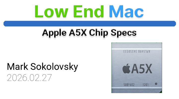
The Apple A5X System on a Chip (SoC) represents a significant milestone in mobile processing technology, specifically designed to power the third-generation iPad. Launched on March 16th, 2012, this dual-core processor, manufactured by Samsung on a 45-nanometer fabrication process, was a crucial component that redefined user experience and performance expectations for tablet computing. Its architecture, featuring a robust CPU and a powerful GPU, was engineered to handle the demanding graphical requirements of Apple’s Retina display and the evolving landscape of mobile applications. This article provides an in-depth examination of the A5X’s technical specifications, its historical context within Apple’s product development, and its broader implications for the consumer electronics market.
Technical Architecture of the Apple A5X
At the heart of the Apple A5X is a dual-core CPU operating at a clock speed of 1 GHz. This processor is based on the ARMv7 instruction set, supporting 32-bit computing. Each of these performance cores is equipped with a 32 KB L1 instruction cache (P-L1i) and a 32 KB L1 data cache (P-L1d), totaling 64 KB for each cache type across the two cores. Furthermore, a unified 1 MB L2 cache is shared between the two performance cores, facilitating faster data access and reducing latency during intensive operations. Unlike later Apple Silicon designs that incorporated efficiency cores for power management, the A5X exclusively focused on performance, indicating its primary role in delivering high-end computing capabilities for its era. The absence of L1 and L2 caches for efficiency cores underscores this singular focus.
The graphical prowess of the A5X was a defining characteristic, particularly its quad-core GPU. This GPU features 8 SIMD Execution Units (EUs) and 64 FP32 ALUs (Arithmetic Logic Units), operating at a clock speed of 200 MHz. This configuration enabled the A5X to deliver an estimated 25.6 GFLOPS (Giga Floating-point Operations Per Second) of processing power, a substantial figure for mobile graphics at the time. This raw graphical horsepower was essential for rendering the high-resolution Retina display of the iPad (2048×1536 pixels), providing smooth animations, detailed visuals, and a more immersive user experience for games and applications. The absence of dedicated AI cores or specific AI processing units in the A5X reflects the nascent stage of artificial intelligence integration in consumer electronics at the time of its release.
Memory management was another critical aspect of the A5X’s design. It utilized a 128-bit memory bus, configured with four channels, each operating at 32-bit width. This setup supported LPDDR2 memory running at 800 MHz (effectively 400 MHz clock speed), contributing to a theoretical memory bandwidth of approximately 12.8 GB/s. The SoC was equipped with 512 MB of RAM, a capacity that was considered generous for mobile devices in 2012 and crucial for handling the large textures and complex data sets required by the Retina display and demanding applications. This high memory bandwidth was instrumental in ensuring that the powerful GPU and CPU had swift access to data, minimizing bottlenecks and maximizing overall system performance.
Historical Context and Market Introduction
The Apple A5X was unveiled as part of the third-generation iPad in March 2012. This launch marked a pivotal moment for Apple and the tablet market. The preceding iPad 2, while successful, did not feature the high-resolution display that had become a hallmark of Apple’s iPhone. The integration of the A5X chip was directly tied to Apple’s ambition to equip its new tablet with a Retina display, a feature that significantly enhanced visual fidelity and set a new standard for mobile screen quality.
The decision to use Samsung as the manufacturer for the A5X was a common practice for Apple during this period, despite ongoing legal disputes between the two companies over intellectual property. Samsung’s advanced manufacturing capabilities were essential for producing the sophisticated chips that powered Apple’s devices. The A5X was an evolution of the A5 chip found in the iPhone 4S and iPad 2, with the primary enhancement being the integration of a significantly more powerful GPU to drive the Retina display. This strategic upgrade highlighted Apple’s commitment to pushing the boundaries of mobile graphics and visual experience.
The release of the third-generation iPad with the A5X was met with considerable anticipation. Reviews at the time often lauded the device’s display quality and performance, with the A5X being credited for enabling a fluid and responsive user interface, even with graphically intensive applications. The chip’s ability to handle the increased pixel count of the Retina display without significant performance degradation was a key differentiator and a testament to Apple’s integrated hardware and software design philosophy.

Broader Impact and Implications
The Apple A5X played a crucial role in solidifying the tablet as a powerful and versatile computing device. Its performance capabilities helped to move tablets beyond simple media consumption devices towards more robust productivity and creative tools. The success of the third-generation iPad, powered by the A5X, further cemented Apple’s dominance in the tablet market and set expectations for future generations of tablets from both Apple and its competitors.
The A5X’s emphasis on graphical performance also had a ripple effect across the mobile app development ecosystem. Developers were encouraged to create more visually rich and graphically demanding applications, knowing that the underlying hardware could support them. This led to advancements in mobile gaming and the development of sophisticated visual design tools for tablets.
Furthermore, the A5X’s architecture, particularly its quad-core GPU and high memory bandwidth, demonstrated Apple’s foresight in anticipating the growing demand for computational power in mobile devices. While the A5X itself was eventually superseded by more advanced Apple Silicon chips, its contribution to the evolution of mobile processing cannot be understated. It showcased the importance of integrating specialized hardware, like powerful GPUs, to meet specific product requirements, a strategy that has become a cornerstone of Apple’s Silicon development.
The A5X’s legacy is intertwined with the rise of the Retina display and the elevation of visual standards in mobile computing. It was a critical component that enabled Apple to deliver a premium user experience, setting a benchmark for performance and visual fidelity that competitors would strive to match. The technical specifications of the A5X, though now dated by current standards, represent a significant step forward in the evolution of mobile SoC design and underscore Apple’s relentless pursuit of innovation in its product offerings. The chip’s development and integration highlight a period of intense competition and rapid advancement in the mobile technology sector, where performance and user experience were paramount.

Analysis of Technical Specifications
The A5X’s dual-core 1 GHz CPU, while not groundbreaking in terms of clock speed by today’s standards, provided sufficient processing power for the tasks expected of a tablet in 2012. The focus was on efficient core design and effective utilization of the ARMv7 architecture. The unified L2 cache of 1 MB was a sensible implementation for a dual-core processor, offering a balance between speed and complexity.
The real standout feature of the A5X was its GPU. The quad-core design, coupled with the specified SIMD EUs and FP32 ALUs, provided a significant leap in graphical performance compared to its predecessors. The 25.6 GFLOPS of theoretical performance were crucial for rendering the high-resolution Retina display, which boasted over 3 million pixels – more than four times the pixel count of the iPad 2’s display. This was a substantial engineering challenge that the A5X was designed to meet.
The memory subsystem was equally critical. The 128-bit memory bus width and the 12.8 GB/s bandwidth were essential for feeding the powerful GPU with the data it needed to render complex graphics at high resolutions. The use of LPDDR2 memory, a common standard at the time, was a practical choice, balancing power consumption, performance, and cost. The 512 MB of RAM was adequate for the operating system and applications of the era, though it would be considered very limited by today’s standards.
The manufacturing process of 45-nanometer was standard for high-performance chips in 2012. Smaller fabrication processes allow for more transistors to be packed into a given area, leading to improved performance and power efficiency. While newer processes have since emerged, 45nm was at the cutting edge for high-volume mobile chip production at the time.

The lack of specific details on transistor count for the A5X in the provided data is not uncommon for Apple’s chips from this era, as Apple often kept such figures proprietary. However, given the complexity of the CPU and GPU cores, along with other integrated components, the transistor count would have been in the tens or hundreds of millions.
The codename "APL5498" and part number "S5L8945" are internal Apple and Samsung identifiers, respectively, that help to track and manage the chip’s development and production. These are typical designations within the semiconductor industry.
Future Developments and Comparisons
The A5X was a stepping stone in Apple’s rapid progression of its A-series chips. It was succeeded by the A6X in the fourth-generation iPad, which featured a custom dual-core CPU and a significantly enhanced GPU, further pushing the boundaries of mobile performance. Apple’s strategy of designing its own silicon, with a focus on custom GPU architectures and tightly integrated memory systems, became a defining characteristic of its products.
The A5X’s technical specifications can be benchmarked against other contemporary mobile processors. While direct comparisons are complex due to differing architectures and optimization strategies, the A5X was generally considered a top-tier mobile SoC for its time, particularly in graphics performance, which was its key selling point for the iPad. Its ability to deliver a smooth Retina display experience was a significant advantage over competitors using less capable graphics hardware.

The evolution from the A5X to subsequent Apple Silicon chips highlights a clear trend towards increased core counts, higher clock speeds, more advanced GPU architectures, and the integration of specialized processing units like Neural Engines for AI tasks. This trajectory has allowed Apple to maintain a performance lead in the mobile and personal computing spaces. The A5X, therefore, serves as an important data point in understanding the historical development of Apple’s highly successful Silicon division.
In conclusion, the Apple A5X was more than just a processor; it was an enabler of a premium user experience that significantly shaped the tablet market. Its robust CPU, exceptionally powerful GPU for its time, and efficient memory architecture combined to deliver the visual fidelity and responsiveness that consumers came to expect from Apple products. The A5X stands as a testament to Apple’s ability to engineer integrated hardware and software solutions that push the boundaries of what is possible in mobile computing.